 中文
中文 English
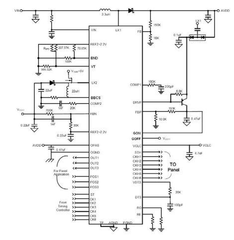
CXLC8988 CXLC8989高性能的升压调节器降压升压控制器高压电荷泵调节器3个VCOM缓冲器(单位增益OPA)开漏拉高VGLC信号发生器和7通道电平移位器有用于有源矩阵薄膜晶体管TFT液晶显示器LCD的可调栅极阴影功能
| 产品型号: | CXLC8988 |
| 产品类型: | 显示屏驱动 |
| 产品系列: | 液晶显示驱动 |
| 产品状态: | 量产 |
| 浏览次数: | 49 次 |
产品简介
技术参数
| 输入电压范围 (VIN) | V ~ 2.6~5.5VV |
|---|---|
| 输出电压 (VOUT) | ADJV |
| 输出电流 (IOUT) | 3A |
| 工作频率 | 600/1200Hz |
| 转换效率 | 95%% |
| 封装类型 | TQFN6X6-48 |
| Dimming method | PSM/PWM |
| Led count | 36×4 |
| Iq | 1UA |
| Interface | 14+1 |
| Power | — |
| Pf value | .9 |
| Topology | 液晶显示驱动 |
| Application type | 显示屏驱动 |
| Topology type | BUCK |
| Protection | OVP/OCP/短路保护 |
| Features | Integrated PMIC for LCD |
| VLX(V) | 20 |
| OPAS/R(V/μs) | 20 |
| OPAISCmA | 200 |
产品详细介绍
目录
7.相关产品
产品概述 返回TOP
The CXLC8988 CXLC8989 includes a high-performance boost regulator, a buck-boost controller, a high voltage charge pump regulator, 3 VCOM buffers (unity-gain OPA), open-drain pull high VGLC signal generator and 7-channel level shifter with adjustable gate shading function for active-matrix thin-film transistor (TFT) liquid-crystal displays (LCDs). The boost regulator provides the regulated supply voltage for the panel source driver ICs. It is a high switching frequency (1.2MHz) current-mode regulator with an integrated 20V/0.1Ω NMOS switch that allows the use of ultra small inductors and ceramic capacitors. It provides fast transient response to pulsed loading while achieving efficiency over 85%. The device can produce output voltage as high as 18V from an input as low as 2.8V. A voltage mode buck-boost controller cooperates with external temperature sensor provide compensated gate-off voltage supply to the level shifters. While the charge pump controller regulates the external charge pump voltage source to supply for the level shifters. The level shifters transform the logic-level control signals generated by the display timing controller (TCON) into the high-level signals needed by LCD panel. Each channel of level shifter output uses low impedance transistors to achieve fast rising and falling time, even when driving the capacitive loads present in LCD applications. Channel 1 to 6 supports gate voltage shading. They are organized in two groups, each with its own shading discharge resistor output. External R-C timer defines shading period though the DTS input. The VCOM buffer can drive the LCD VCOM voltage that features high short-circuit current (200mA), fast slew rate (20V/μs), wide bandwidth (8MHz) and rail-to-rail input/output.
产品特点 返回TOP
„ 2.6V~5.5V Supply Range
„ Current Mode Boost Regulator for AVDD
Š 0.1Ω/20V/3A Embedded NMOS switch
Š Fixed 1.2MHz Switching Frequency
Š Up to 85% Efficiency
Š 1% Output Regulation
„ Voltage Mode Buck-Boost Regulator for VGOFF
Š Fixed 600kHz Switching Frequency
Š Up to 85% Efficiency
Š 1% Output Regulation
„ Charge Pump Regulator for VGON
„ 3-Channel Rail-to-Rail Unity-Gain Operational Amplifier
Š ±200mA Output Short Circuit Current
Š 20V/μs Slew Rate
Š 18MHz, -3dB Bandwidth
„ Built-In Power On Sequence and Soft Start Function
„ 7-Channel Level Shifter
Š +33V Highest Voltage Level
Š -30V Lowest Voltage Level
Š Maximum 1μs Rising/Falling Time
Š 300mA Peak Current
Š 15mA Continuous Current
Š Adjustable Gate Shading Function
„ Opened Drain Pull High VGLC Signal
„ Protections:
Š Input Under Voltage Lockout (UVLO)
Š Over Current Protection for AVDD (OCP)
Š Output Under Voltage Protection for AVDD, GON and GOFF (UVP)
Š Output Over Voltage Protection for AVDD, GON and GOFF (OVP)
Š Operational Amplifier Short Circuit Protection (SCP)
Š Over Temperature Protection (OTP)
„ TQFN6x6-48L Package
„ RoHS Compliant
应用范围 返回TOP
„ LCD TV Panel
„ LCD Monitor Panel
技术规格书(产品PDF) 返回TOP
需要详细的PDF规格书请扫一扫微信联系我们,还可以获得免费样品以及技术支持!

产品封装图 返回TOP

电路原理图 返回TOP
相关芯片选择指南 返回TOP 更多同类产品......
|
Integrated PMIC for LCD |
|||||||||
|
Part NO. |
Vin(V) min. |
Vin(V) max. |
FSW (kHz) |
ILX (A) |
VLX (V) |
OPAS/ R(V/μs |
OPAI SCmA |
Note |
Package |
|
2.5 |
5.5 |
1200 |
3 |
18 |
40 |
200 |
Async-Boost,VGH/VGL Charge-Pump, VCOM,GPM, Voltage Detector |
TQFN4X4-24 |
|
|
2.5 |
5.5 |
1200 |
1.8 |
20 |
12 |
150 |
Async-Boost, VCOM,VGH/VGL Charge-Pump, 1-CH WLED Driver with EN,LXB=20V/1.2A |
TQFN4X4-24 |
|
|
2.5 |
5.5 |
1200 |
2 |
20 |
12 |
200 |
Async-Boost,VGL Regulator,LDO,GPM,OPA, Voltage Detector,6-CH WLED Driver,30mA/CH |
TQFN5X5-40 |
|
|
2.5 |
5.5 |
600 |
2 |
20 |
12 |
200 |
Async-Boost,VGL Regulator,LDO,GPM,OPA, Voltage Detector,6-CH WLED Driver,30mA/CH |
TQFN5X5-40 |
|
|
2.6 |
5.5 |
600/ 1200 |
3 |
20 |
20 |
200 |
Async-Boost,VGH Regulator,OPA*3,Buck-Boost VGL Temp. Compensation,7-CH-33V~+33V Level-Shifter |
TQFN6X6-48 |
|
|
2.6 |
5.5 |
600/ 1200 |
-- |
-- |
20 |
200 |
Async-Boost,VGH Regulator,OPA*3,Buck-Boost VGL Temp. Compensation,7-CH-33V~+33V Level-Shifter |
QFN6X6-48 |
|
|
2.6 |
5.5 |
600/ 1200 |
3 |
20 |
20 |
200 |
Async-Boost,VGH Regulator,OPA*3,Buck -Boost VGL with Temp. Compensation |
QFN5X5-32 |
|
|
8 |
14 |
750 |
5 |
24 |
30 |
200 |
Async-Boost,Async-Buck, OPA,VGON and VGOFF Regulator,GPM,VGH Temp. Compensation,I2C |
TQFN6X6-40 |
|
|
2.5 |
5.5 |
1200 |
4.5 |
18 |
-- |
-- |
Async-Boost, VGHM,VGH/VGOFF Charge-Pump |
TQFN5X5-20 |
|
|
2.5 |
5.5 |
1200 |
3 |
18 |
40 |
200 |
Async-Boost,VGH/VGL Charge-Pump, VCOM, GPM,Voltage Detector |
TQFN4X4-24 |
|
|
2.5 |
5.5 |
1200 |
1.8 |
20 |
12 |
150 |
Async-Boost,VGH/VGL Charge-ump,VCOM, CXLC8994A With EN,CXLC8994S With XAO |
TQFN3X3-16 |
|
|
2.5 |
5.5 |
1200 |
1.8 |
20 |
12 |
150 |
Async-Boost,VGH/VGL Charge-Pump,VCOM, CXLC8994A With EN,CXLC8994S With XAO |
TQFN3X3-16 |
|
|
2.5 |
5.5 |
640/ 1200 |
2 |
20 |
12 |
150 |
Async-Boost, VGH Charge-Pump,VCOM, GPM, Voltage Detector,LDO |
TQFN4X4-24 |
|
|
2.5 |
5.5 |
640/ 1200 |
2 |
20 |
12 |
150 |
Async-Boost,VGH Charge-Pump,VCOM,LDO,GPM, Voltage Detector,4-CH WLED Driver,50mA/CH |
TQFN5X5-40 TQFN3.8X6.2 |
|
|
2.5 |
5.5 |
640/ 1200 |
2 |
20 |
12 |
150 |
Async-Boost,VGH Charge-Pump,VCOM, GPM, Voltage Detector |
TQFN4X4-24 |
|
|
2.5 |
5.5 |
1200 |
1.8 |
20 |
12 |
150 |
Async-Boost,VGH Charge-Pump,VGL Charge-Pump, Voltage Detector,1-CH WLEDdriver,240mA/CH,HVInput |
TQFN4X4-24 |
|
|
8 |
14 |
500/ 750 |
2.3 |
19 |
-- |
-- |
Async-Boost,Async-Buck,VGH/VGL,Charge-Pump |
TSSOP-28(FD) |
|
|
8 |
14 |
500/ 750 |
3 |
20 |
45 |
200 |
Async-Boost,Async-Buck, VGH/VGL Charge-Pump, GPM,VCOM,Voltage Detector,HV LDO |
TQFN7X7-48 |
|
|
9.5 |
14 |
500~ 2000 |
3.5 |
20 |
-- |
-- |
Async-Boost,Async-Buck,VGON and VGOFF Regulator |
TQFN5X5-28 |
|
|
8 |
14 |
750/ 1000 |
5 |
24 |
-- |
-- |
Async-Boost,Sync-Buck*2,Async-Buck,VGON and VGOFF Regulator,GPM,VGH Temp.Compensation,I2C |
TQFN6X6-40 |
|

用户评论