 中文
中文 English
CXSD62121 VTT的输出电压只需要20μF的陶瓷输出电容就可以稳定和快速的瞬态响应
目录
1.产品概述 2.产品特点
3.应用范围 4.下载产品资料PDF文档
5.产品封装图 6.电路原理图
7.功能概述 8.相关产品
一,产品概述(General Description)
The CXSD62121A CXSD62121B CXSD62121 integrates a synchronous buck PWM con-troller to generate VDDQ, a sourcing and sinking LDO linear regulator to generate VTT. It offers the lowest total solution cost in system where space is at a premium. The CXSD62121A CXSD62121B CXSD62121 provides excellent transient response and accurate DC voltage output in either PFM or PWM Mode.In Pulse Frequency Mode (PFM), the CXSD62121A CXSD62121B CXSD62121 provides very high efficiency over light to heavy loads with loading-modulated switching frequencies. On TQFN-20 Package,the Forced PWM Mode works nearly at constant frequency for low-noise requirements. The CXSD62121A CXSD62121B CXSD62121 is equipped with accurate current-limit,output under-voltage, and output over-voltage protections.A Power-On- Reset function monitors the voltage on VCC prevents wrong operation during power on. Droop func-tion is allowed to adjust output voltage during light load period.The LDO is designed to provide a regulated voltage with bi-directional output current for DDR-SDRAM termination.The device integrates two power transistors to source or sink current up to 1.5A. It also incorporates current-limit and thermal shutdown protection.The output voltage of LDO tracks the voltage at VREF pin.An internal resistor divider is used to provide a half volt-age of VREF for VTTREF and VTT Voltage. The VTT output voltage is only requiring 20μF of ceramic output capaci tance for stability and fast transient response. The S3 and S5 pins provide the sleep state for VTT (S3 state)and suspend state (S4/S5 state) for device, when S5 and S3 are both pulled low the device provides the soft-off for VTT and VTTREF
产品特点(Features)
High Input Voltages Range from 3V to 28V Input Power
Provide Adjustable Output Voltage from 0.75V to
5.5V +1% Accuracy over Temperature
Integrated MOSFET Drivers and Bootstrap Forward P-CH MOSFET
Low Quiescent Current (200μA)
Excellent Line and Load Transient Responses
PFM Mode for Increased Light Load Efficiency
Constant On-Time Controller Scheme
- Switching Frequency Compensation for PWM Mode
- Adjustable Switching Frequency from 100kHz to
550kHz in PWM Mode with DC Output Current
S3 and S5 Pins Control The Device in S0, S3 or S4/S5 State
Power Good Monitoring
Extra Droop Voltage Control Function with
Adjustable Current Setting
70% Under-Voltage Protection (UVP)
125% Over-Voltage Protection (OVP)
Adjustable Current-Limit Protection
- Using Sense Low-Side MOSFET’s RDS(ON)
TQFN-20 3mmx3mm Thin package
Lead Free Available (RoHS Compliant)
+1.5A LDO Section (VTT)
Sourcing or Sinking Current up to 1.5A
Fast Transient Response for Output Voltage
Output Ceramic Capacitors Support at least 10μF MLCC
VTT and VTTREF Track at Half the VDDQSNS by internal divider
+20mV Accuracy for VTT and VTTREF
Independent Over-Current Limit (OCL)
Thermal Shutdown Protection
三,应用范围 (Applications)
DDR2, and DDR3 Memory Power Supplies
SSTL-2 SSTL-18 and HSTL Termination
四.下载产品资料PDF文档
需要详细的PDF规格书请扫一扫微信联系我们,还可以获得免费样品以及技术支持!

五,产品封装图 (Package)

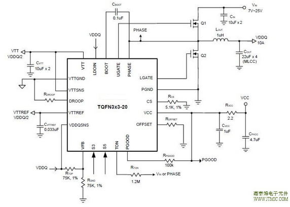
六.电路原理图

七,功能概述
Soft- Start (cont.)
During soft-start stage before the PGOOD pin is ready,
the under voltage protection is prohibited. The over volt-
age and current limit protection functions are enabled. If
the output capacitor has residue voltage before startup,
both low-side and high-side MOSFETs are in off-state
until the internal digital soft start voltage equal the inter-
nal feedback voltage. This will ensure the output voltage
starts from its existing voltage level.
The VTT LDO part monitors the output current, both sourc-
ing and sinking current, and limits the maximum output
current to prevent damages during current overload or
short circuit (shorted from VTT to GND or VLDOIN)
conditions.
The VTT LDO provides a soft-start function, using the
constant current to charge the output capacitor that gives
a rapid and linear output voltage rise. If the load current is
above the current limit start-up, the VTT cannot start
successfully.CXSD62121A CXSD62121B CXSD62121 has an independent counter for each output,
but the PGOOD signal indicates only the status of VDDQ
and does not indicate VTT power good externally.
Power-Good Output (PGOOD)
PGOOD is an open-drain output and the PGOOD com-
parator continuously monitors the output voltage. PGOOD
is actively held low in shutdown, and standby. When PWM
converter’s output voltage is greater than 95% of its tar-
get value, the internal open-drain device will be pulled
low. After 63μs debounce time, the PGOOD goes high.
The PGOOD goes low if VVDDQ output is 10% below or
above its nominal regulation point.
Under Voltage Protection
In the process of operation, if a short-circuit occurs, the
output voltage will drop quickly. When load current is big-
ger than current limit threshold value, the output voltage
will fall out of the required regulation range. The under-
voltage continually monitors the setting output voltage
after 2ms of PWM operations to ensure startup. If a load
step is strong enough to pull the output voltage lower
than the under voltage threshold (70% of normal output
voltage), CXSD62121A CXSD62121B CXSD62121 shuts down the output gradually and
latches off both high and low side MOSFETs.
Over Voltage Protection (OVP)
The feedback voltage should increase over 125% of the
reference voltage due to the high-side MOSFET failure or
for other reasons, and the over voltage protection com-
parator designed with a 1.5μs noise filter will force the
low-side MOSFET gate driver to be high. This action ac-
tively pulls down the output voltage and eventually at-
tempts to blow the battery fuse.
When the OVP occurs, the PGOOD pin will pull down and
latch-off the converter. This OVP scheme only clamps the
voltage overshoot, and does not invert the output voltage
when otherwise activated with a continuously high output
from low-side MOSFET driver. It’s a common problem for
OVP schemes with a latch. Once an over-voltage fault
condition is set, toggling VCC power-on-reset signal can
only reset it.
PWM Converter Current Limit
The current-limit circuit employs a unique “valley” current
sensing algorithm (Figure 2). CS pin should be con-
nected to VCC through the trip voltage-setting resistor,
RCS. CS terminal sinks 5mA current, ICS, and the current
limit threshold is set to the voltage across the RCS. The
voltage between or CS_GND pin and PHASE pin moni-
tors the inductor current so that PHASE pin should be
connected to the drain terminal of the low side MOSFET.
PGND is used as the positive current sensing node so
that PGND should be connected to the proper current
sensing device, i.e. the sense resistor or the source ter-
minal of the low side MOSFET.
If the magnitude of the current-sense signal is above the
current-limit threshold, the PWM is not allowed to initiate
a new cycle. The actual peak current is greater than the
current-limit threshold by an amount equal to the induc-
tor ripple current. Therefore, the exact current- limit char-
acteristic and maximum load capability are a function of
the sense resistance, inductor value, and input voltage.
八,相关产品 更多同类产品......
|
Switching Regulator > Buck Controller |
||||||||||
|
Part_No |
Package |
Archi tectu |
Phase |
No.of PWM Output |
Output Current (A) |
Input Voltage (V) |
Reference Voltage (V) |
Bias Voltage (V) |
Quiescent Current (uA) |
|
|
min |
max |
|||||||||
|
SOP-14 QSOP-16 QFN4x4-16 |
VM |
1 |
1 |
30 |
2.9 |
13.2 |
0.9 |
12 |
8000 |
|
|
SOP-8 |
VM |
1 |
1 |
20 |
2.9 |
13.2 |
0.8 |
12 |
5000 |
|
|
SOP-8 |
VM |
1 |
1 |
20 |
2.9 |
13.2 |
0.8 |
12 |
5000 |
|
|
QFN4x4-24 |
VM |
2 |
1 |
60 |
3.1 |
13.2 |
0.6 |
12 |
5000 |
|
|
SOP-8 |
VM |
1 |
1 |
20 |
2.2 |
13.2 |
0.8 |
5~12 |
2100 |
|
|
SOP-8 |
VM |
1 |
1 |
20 |
2.2 |
13.2 |
0.8 |
5~12 |
2100 |
|
|
SOP8|TSSOP8 |
VM |
1 |
1 |
5 |
5 |
13.2 |
1.25|0.8 |
5~12 |
3000 |
|
|
SOP-8 |
VM |
1 |
1 |
10 |
3.3 |
5.5 |
0.8 |
5 |
2100 |
|
|
SOP-14 |
VM |
1 |
1 |
10 |
5 |
13.2 |
0.8 |
12 |
2000 |
|
|
TSSOP-24 |QFN5x5-32 |
VM |
1 |
2 |
20 |
5 |
13.2 |
0.6 |
5~12 |
4000 |
|
|
SOP14 QSOP16 QFN-16 |
VM |
1 |
1 |
30 |
2.9 |
13.2 |
0.9 |
12 |
4000 |
|
|
SOP-14 |
VM |
1 |
1 |
30 |
2.2 |
13.2 |
0.6 |
12 |
5000 |
|
|
SOP-14 |
VM |
1 |
1 |
30 |
2.2 |
13.2 |
0.6 |
12 |
5000 |
|
|
SOP-14 |
VM |
1 |
1 |
25 |
2.2 |
13.2 |
0.8 |
12 |
5000 |
|
|
LQFP7x7 48 TQFN7x7-48 |
VM |
1 |
6 |
0.015 |
1.4 |
6.5 |
- |
5 |
1800 |
|
|
TSSOP-24P |
VM |
1 |
2 |
20 |
2.97 |
5.5 |
0.8 |
5~12 |
5000 |
|
|
SOP-14 |
VM |
1 |
1 |
10 |
5 |
13.2 |
||||


发表评论