同步buck-PWM控制器2-a源线性调节器和缓冲基准CXSD62355用于DDR2 DDR3和DDR3L内存系统同步降压控制器VDDQ

目录
7.相关产品
产品概述 返回TOP
The CXSD62355 is intended for DDR2, DDR3 and DDR3L memory systems. It integrates a synchronous buck PWM controller with a 2-A sink-source linear regulator and buffered reference. The PWM controller uses constant on-time control scheme to handle wide input/output voltage ratios with ease and provides 100ns “instant-on” response to load transients while maintaining a relatively constant switching frequency. The CXSD62355 achieves high efficiency at a reduced cost by eliminating the current-sense resistor found in traditional current-mode PWMs. Efficiency is further enhanced by an ability to drive very large synchronous rectifier MOSFETs. Single-stage buck conversion allows these devices to directly step down high-voltage batteries for the highest possible efficiency. The 2A sink/source tracking termination regulator is specifically designed for low-cost/ low-external component count systems. The regulator contains a high speed operational amplifier that provides fast load transient response with only 10μF of ceramic output capacitance. The CXSD62355 supports remote sensing functions and all features required to power the DDR2 /DDR3 /DDR3L VTT bus termination according to the JEDEC specification. In addition, the CXSD62355 includes integrated sleep-state controls placing VTT in High-Z in S3 (suspend to RAM) and soft-off for VTT and VTTREF in S4/S5 (Shutdown). The CXSD62355 provides OVP, UVP, over current and thermal shutdown protection functions and is available in a 20-pin 3X3 TQFN package.
产品特点 返回TOP
•Synchronous Buck Controller (VDDQ)
„ Ultra-High Efficiency at Light and Heavy Load with Auto-skip Function „ No Current-Sense Resistor (Lossless ILIMIT)
„ Quasi-PWM with 100ns Load-Step Response
„ 0.7V to 1.8V Adjustable Output Range
„ 3V to 28V Battery Input Range
„ 0.8% Vref Accuracy
„ Supports Soft-off in S4/S5 States
„ Selectable 300k/400kHz Switching Frequency
„ OVP & UVP of VDDQ Output
„ Drives Large Synchronous-Rectifier FETs
„ Power-Good Indicator
•2-A LDO (VTT), Buffered Reference (VTTREF)
„ VLDOIN Voltage Range: 1.2 V to 3.6 V
„ Requires Only 10μF Ceramic VTT Output Capacitance
„ Supports High-Z in S3 and Soft-Off in S4/S5
„ Integrated Divider Tracks 1/2 VDDQSNS for Both VTT and VTTREF
„ Remote Sensing (VTTSNS)
„ ±20mV VTT and 0.8% VTTREF Accuracy
„ 10mA Buffered Reference (VTTREF)
„ Built-In Soft-Start to Reduce the VLDOIN Surging Current
„ Over Current Protection of VTT Output
„ Thermal Shutdown Protection
应用范围 返回TOP
„ Notebook Computers
„ CPU Core Supply
„ Chipset/RAM Supply as Low as 0.7V
技术规格书(产品PDF) 返回TOP
需要详细的PDF规格书请扫一扫微信联系我们,还可以获得免费样品以及技术支持!

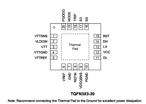
产品封装图 返回TOP

电路原理图 返回TOP
a
相关芯片选择指南 返回TOP 更多同类产品......
|
Synchronous (Quasi-PWM) Step Down Controller |
|||||||
|
Part NO. |
Vin(V) min. |
Vin(V) max. |
VOUT (V) |
FSW (k Hz) |
FB (V) |
Note |
Package |
|
3 |
28 |
0.7~1.8 |
300/400 |
0.8 |
EN, SS, PGOOD, OVP, UVP, OCP, VTTREF, Built-in BST diode, DDR1/2/3/3L, 2A LDO for VTT |
TQFN3X3-20 |
|
|
4.5 |
28 |
0.7~2.6 |
ADJ |
0.7 |
EN, PGOOD, OVP, UVP, OCP, VOUT Adjustable,1.5ms VOUT Servo Soft Start, 4700ppm/°C RON Coefficient |
TDFN3X3-10 |
|
|
4.5 |
28 |
0.5~3.3 |
ADJ |
0.5 |
EN, PGOOD, OVP, UVP, OCP, VOUT Adjustable, 1.5ms VOUT Servo Soft Start, 4700ppm/°C RON Coefficient |
TQFN2X2-12 |
|
|
4.5 |
24 |
0.75~3.6 |
ADJ |
0.75 |
EN, SS, PGOOD, OVP, UVP, OCP, Built-in BST diode |
TQFN3X3-16 |
|
|
4.5 |
24 |
0.75~3.6 |
ADJ |
0.75 |
EN, SS, PGOOD, OVP, UVP, OCP, Built-in BST diode |
TQFN3X3-16 |
|
|
4.5 |
24 |
0.75~3.6 |
ADJ |
0.75 |
EN, SS, PGOOD, OVP, UVP, OCP, Built-in BST diode |
TQFN3X3-16/TQFN3.5X3.5-14 |
|
|
2 |
24 |
0.75~3.6 |
400/ADJ |
0.75 |
EN, SS, PGOOD, OVP, UVP, OCP, VTTREF, Built-in BST diode, DDR1/2/3/3L, 3A/2A LDO for VTT |
TQFN4X4-24/TQFN3X3-20 |
|
|
4.5 |
24 |
0.75~3.6 |
ADJ |
0.75 |
EN, PGOOD, OVP, UVP, OCP, Built-in BST diode, SS, G0 & G1 Controls VOUT |
TQFN3X3-16 |
|

 中文
中文 English

发表评论