 中文
中文 English
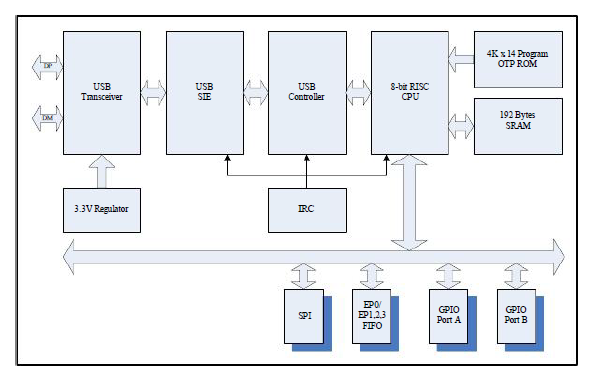
CXUS7717内置USB收发器和3.3V调节器支持USB暂停和恢复功能全速和低速USB 1.1规格PS2兼容接口与USB接口共享通用可编程IO级接口内部时钟发生器8位RISC CPU核心
| 产品型号: | CXUS7717 |
| 产品类型: | 通用MCU |
| 产品系列: | 通用微控制器MCU |
| 产品状态: | 量产 |
| 浏览次数: | 36 次 |
产品简介
支持全速和低速USB 1.1规格。
内置USB收发器和3.3V调节器。
支持USB暂停和恢复功能。
一个控件输入/输出,三个INT(输入/输出)/Bulk(输入/输出)端点。
支持PS2兼容接口与USB接口共享。
192字节内部SRAM。
4K x 14内部程序OTP-ROM
8位RISC CPU核心。
支持主/从SPI串行通信接口。
最多支持三个用户配置的终结点。
最多三个64字节数据终结点(EP0、EP1、EP2、EP3)。
内部时钟发生器
0.25%准确度。
提供24MHz或16MHz或12MHz时钟输出。
通用可编程IO级接口。
仅5V电源;GPIO支持1.8V~5.5V接口。
提供3.3V电压。
支持SSC降低EMI。
技术参数
| 输入电压范围 (VIN) | ≤ 2.7~5.5VV |
|---|---|
| 输出电流 (IOUT) | 45mAA |
| Core | USB MODE:INT/BULK |
| Main frequency | Stack:8 |
| Flash | 4K(OTP) |
| Ram | 192 |
| Peripherals | EP0 IN:64Byte, EP0 OUT:64Byte |
| Features | EP1 IN:64ByteEP1 OUT:64Byte |
| Application | EP2 IN:64ByteEP2 OUT:64Byte |
产品详细介绍
目录
1.产品概述 2.产品特点 3.应用范围 4.技术规格书下载(PDF文档)
一.产品概述
The CXUS7717 has program memory size greater 2K works, but the CALL and GOTO instructions only have a 11-bits address range. This 11-bit address range allows a branch within a 2K program memory page size. To allow CALL and GOTO instructions to address the entire 4K program memory address range for CX8U83M, there is another two bits to specify the program memory page. The paging bit comes from the ROMBANK bit (PUMODE[5]). When doing a CALL or GOTO instruction, the user must ensure that page bit ROMBANK are programmed so that the desired program memory page is addressed. When one of return instructions is executed, the entire 12-bit PC is POPed from the stack. Therefore, manipulation of the ROMBANK is not required for return instructions.
二.产品特点
Support Full-Speed and Low-Speed USB 1.1 specification.
Built-in USB Transceiver and 3.3V regulator.
Support USB Suspend and Resume function.
One Control IN/OUT, three INT (IN/OUT) /Bulk (IN/OUT) endpoints.
Support PS2 compatible interface share with USB interface.
192 bytes internal SRAM.
4K x 14 internal program OTP-ROM
8-bit RISC CPU core.
Support Master/Slave SPI serial Communication Interface.
Support up to three user configured endpoints.
Up to three 64-byte data endpoints (EP0, EP1, EP2, EP3).
Internal Clock Generator
0.25% Accuracy.
Supply 24MHz or 16MHz or 12MHz clock output.
General-purpose programmable-level IO interface.
5V power supply only; GPIO support 1.8V~5.5V interface.
Supply 3.3V voltage.
Support SSC to reduce EMI.
三.应用范围
CXUS7717 enhance PS2 mode and I/O voltage support to 1.8V~5.5V
CXUS7717 functional and coding is compatible to CX8PU83S.
CXUS7717 configuration option table, please reference page-6
四.技术规格书(产品PDF)
需要详细的PDF规格书请扫一扫微信联系我们,还可以获得免费样品以及技术支持!

五.产品封装图

六.电路原理图
七.相关芯片选择指南 更多同类产品......
|
USB |
|||||||||||||||||
|
Product |
OTP |
RAM |
I/O |
I/O |
3.3V |
USB |
Stack |
EP0 |
EP1 |
EP2 |
EP3 |
EP4 |
|||||
|
ROM |
Byte |
Voltage |
OUT |
MODE |
|||||||||||||
|
Range |
IN |
OUT |
IN |
OUT |
IN |
OUT |
IN |
OUT |
IN |
OUT |
|||||||
|
4K(OTP) |
192 |
14 |
1.8V~5.5V |
45mA |
INT/BULK |
8 |
64Byte |
64Byte |
64Byte |
64Byte |
64Byte |
64Byte |
64Byte |
64Byte |
NA |
NA |
|
|
6K(OTP) |
192 |
16 |
1.8V~5.5V |
45mA |
INT/BULK |
5 |
8Byte |
8Byte |
8Byte |
NA |
8Byte |
NA |
32Byte |
NA |
NA |
32Byte |
|
|
6K(OTP) |
192 |
16 |
1.8V~5.5V |
45mA |
INT/BULK |
5 |
8Byte |
8Byte |
8Byte |
NA |
8Byte |
||||||

用户评论