 中文
中文 English
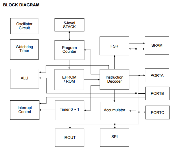
CX8PE59E CX8PE59可直接或间接寻址其寄存器文件和数据存储器8位宽数据通道5层深度硬件堆栈4K x 13位片上EPROM/ROM144 x 8位片上通用寄存器SRAM内部通电复位POR看门狗启用禁用控制
| 产品型号: | CX8PE59E |
| 产品类型: | 通用MCU |
| 产品系列: | 通用微控制器MCU |
| 产品状态: | 量产 |
| 浏览次数: | 0 次 |
产品简介
·只有49条单字指令
·所有指令都是单周期的,除了两个周期的程序分支
·13位宽指令
·所有ROM/EPROM区域GOTO/FGOTO指令
·所有ROM/EPROM区域子程序调用/FCALL指令
·8位宽数据通道
·5层深度硬件堆栈
·4K x 13位片上EPROM/ROM
·144 x 8位片上通用寄存器(SRAM)
·工作速度:DC-20MHz时钟输入DC-100ns指令周期
·数据访问的直接、间接寻址模式
·一个8位实时时钟/计数器(定时器0),带8位可编程预分频器
·一个8位实时时钟/计数器(Timer1),带2位可编程预分频器和周期设置
·内部通电复位(POR)
·内置低压探测器(LVD),用于褐化复位(BOR)
·通电复位定时器(PWRT)和振荡器启动定时器(OST)
·带内部振荡器的片上看门狗定时器(WDT),用于可靠操作和软件看门狗启用/禁用控制
·三个具有独立方向控制的I/O端口IOA、IOB和IOC
·16个软件控制拉高引脚:端口B/端口C
·8个软件控制下拉销:IOA0~A3/IOB0~B3
·2个软件控制开漏引脚:IOC6/IOC7
·具有可编程频率和占空比的红外输出通道
串行外围接口(SPI)
·四个内部中断源:定时器0溢出、定时器1匹配、IROUT和SPI模块;两个外部中断源:INT0引脚和INT1引脚
·从睡眠中醒来,端口B/IOC4/IOC5输入下降
·省电睡眠模式
·可编程代码保护
·可选振荡器选项:
-外部电阻/电容振荡器
-XT:晶体/谐振器振荡器
-高频晶体/谐振器振荡器
-低频晶体振荡器
-IRC:内部电阻/电容振荡器
·宽工作电压范围:
-EPROM:2.3V至5.5V
-ROM:2.3V至5.5V
技术参数
| 输入电压范围 (VIN) | ≤ 1.8~5.5VV |
|---|---|
| 封装类型 | DIP/SOP/SSOP28/DIP/SOP32 |
| Core | Int.:4 |
| Main frequency | Ext. Inte.:2 |
| Flash | 4K(OTP) |
| Ram | 144 |
| Peripherals | 24 |
| Features | Stack:5 |
| Application | ADC:No |
产品详细介绍
目录
产品概述 返回TOP
The CX8PE59 series is a family of low-cost, high speed, high noise immunity, EPROM/ROM-based 8-bit CMOS microcontrollers. It employs a RISC architecture with only 47 instructions. All instructions are single cycle except for program branches which take two cycles. The easy to use and easy to remember instruction set reduces development time significantly. The CX8PE59 series consists of Power-on Reset (POR), Brown-out Reset (BOR), Power-up Reset Timer (PWRT), Oscillator Start-up Timer(OST), Watchdog Timer, EPROM/ROM, SRAM, tri-state I/O port, I/O pull-high/open-drain/pull-down control, Power saving SLEEP mode, 2 real time programmable clock/counter, Interrupt, IROUT, SPI, Wake-up from SLEEP mode, and Code Protection for EPROM products. There are four oscillator configurations to choose from, including the power-saving LP (Low Power) oscillator and cost saving RC oscillator. The CX8PE59 series address 4K×13 of program memory. The CX8PE59 series can directly or indirectly address its register files and data memory. All special function registers including the program counter are mapped in the data memory.
产品特点 返回TOP
‧ Only 49 single word instructions
‧ All instructions are single cycle except for program branches which are two-cycle
‧ 13-bit wide instructions
‧ All ROM/EPROM area GOTO/FGOTO instruction
‧ All ROM/EPROM area subroutine CALL/FCALL instruction
‧ 8-bit wide data path
‧ 5-level deep hardware stack
‧ 4K x 13 bits on chip EPROM/ROM
‧ 144 x 8 bits on chip general purpose registers (SRAM)
‧ Operating speed: DC-20 MHz clock input DC-100 ns instruction cycle
‧ Direct, indirect addressing modes for data accessing
‧ One 8-bit real time clock/counter (Timer0) with 8-bit programmable prescaler
‧ One 8-bit real time clock/counter (Timer1) with 2-bit programmable prescaler and period setting
‧ Internal Power-on Reset (POR)
‧ Built-in Low Voltage Detector (LVD) for Brown-out Reset (BOR)
‧ Power-up Reset Timer (PWRT) and Oscillator Start-up Timer(OST)
‧ On chip Watchdog Timer (WDT) with internal oscillator for reliable operation and soft-ware watch-dog enable/disable control
‧ Three I/O ports IOA, IOB and IOC with independent direction control
‧ 16 soft-ware control pull-high pins: Port B/Port C
‧ 8 soft-ware control pull-down pins:IOA0~A3/IOB0~B3
‧ 2 soft-ware control open-drain pins: IOC6/IOC7
‧ IR output channel with programmable frequency and duty cycle
‧ Serial Peripheral Interface (SPI)
‧ Four internal interrupt source: Timer0 overflow, Timer1 match, IROUT, and SPI module; Two external interrupt source: INT0 pin, and INT1 pin
‧ Wake-up from SLEEP by Port B/IOC4/IOC5 input falling
‧ Power saving SLEEP mode
‧ Programmable Code Protection
‧ Selectable oscillator options:
- ERC: External Resistor/Capacitor Oscillator
- XT: Crystal/Resonator Oscillator
- HF: High Frequency Crystal/Resonator Oscillator
- LF: Low Frequency Crystal Oscillator
- IRC: Internal Resistor/Capacitor Oscillator
‧ Wide-operating voltage range:
- EPROM : 2.3V to 5.5V
- ROM : 2.3V to 5.5V
应用范围 返回TOP
a
技术规格书(产品PDF) 返回TOP
需要详细的PDF规格书请扫一扫微信联系我们,还可以获得免费样品以及技术支持!

产品封装图 返回TOP

电路原理图 返回TOP
相关芯片选择指南 返回TOP 更多同类产品......
|
GPIO |
|||||||||||||||
|
Product Name |
ROM |
RAM |
I/O |
Ext. |
Int. |
Wake up |
Stack |
Timer |
PWM / |
ADC |
LCD |
Interface |
IRC |
Package |
Status |
|
(Word) |
(Byte) |
Inte. |
Int. |
IROUT |
|||||||||||
|
4K(MASK ROM) |
140 |
38 |
1 |
7 |
Yes |
5 |
8bit*4 |
10bit PWM*2 |
15bit RFC*19 |
No |
SPI |
No |
DIP40/QFP44 |
MP |
|
|
4(MASK ROM) |
144 |
24 |
2 |
1 |
Yes |
5 |
8bit*1 |
No |
No |
No |
No |
Yes |
DIO/SOP |
MP |
|
|
4K(OTP) |
140 |
38 |
1 |
7 |
Yes |
5 |
8bit*4 |
10bit PWM*2PWM*2 |
15bit RFC*19 |
No |
SPI |
No |
DIP40/QFP44 |
MP |
|
|
1K(OTP) |
49 |
16 |
2 |
1 |
Yes |
5 |
8bit*1 |
No |
No |
No |
No |
Yes |
DIP/SOP18/SSOP20 |
MP |
|
|
512(OTP) |
48 |
20 |
1 |
1 |
Yes |
5 |
8bit*1 |
No |
No |
No |
No |
Yes |
DIP/SOP/SSOP28 |
MP |
|
|
2K(OTP) |
96 |
20 |
1 |
1 |
Yes |
5 |
8bit*1 |
No |
No |
No |
No |
Yes |
DIP/SOP/SSOP28 |
MP |
|
|
4K(OTP) |
144 |
24 |
2 |
4 |
Yes |
5 |
8bit*2 |
IROUT |
No |
No |
SPI |
Yes |
DIP/SOP/SSOP2 8/DIP/SOP32 |
MP |
|
|
1K(OTP) |
49 |
12 |
2 |
1 |
Yes |
5 |
8bit*1 |
No |
No |
No |
No |
Yes |
DIP14/SOP14 |
MP |
|
|
1K |
49 |
16 |
2 |
1 |
Yes |
5 |
8bit*1 |
No |
No |
No |
No |
Yes |
DIP/SOP18 |
MP |
|
|
1K(OTP) |
49 |
12 |
2 |
1 |
Yes |
5 |
8bit*1 |
No |
No |
No |
No |
Yes |
DIP14/SOP1 |
||

用户评论