 中文
中文 English
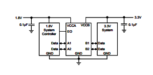
CXCO4332在通电或断电期间的高阻抗状态EO应通过下拉电阻器连接到GND电阻器的最小值由驱动器的电流源能力决定4位非垂直转换器使用两个单独的可配置电源轨
| 产品型号: | CXCO4332 |
| 产品类型: | ADC/DAC |
| 产品系列: | 逻辑电路比较器 |
| 产品状态: | 量产 |
| 浏览次数: | 49 次 |
产品简介
·端口1.2V至3.6V,B端口1.65V至5.5V(VCCA≤VCCB)
·VCC隔离特性如果任一VCC输入处于GND,则所有输出均处于高阻抗状态
·参考VCCA的EO输入电路
低功耗,最大5μA ICC
·无需电源顺序,VCCA或VCCB可先倾斜
“关闭”支持部分断电模式操作
·锁存性能超过100毫安/JESD 78,II级
·ESD保护超过JESD 22–A端口2500V人体模型(A114-B)1500V充电装置模型(C101)–B端口±15kV人体模型(A114-B)1500V充电装置模型(C101)
技术参数
| 输入电压范围 (VIN) | ≤ 1.2~5.5VV |
|---|---|
| 输出电压 (VOUT) | adjV |
| 输出电流 (IOUT) | 500mAA |
| 工作频率 | 1MHz Hz |
| 转换效率 | 93%% |
| 封装类型 | SC-70-6/SOT-23-6/AQFN1.7X2.0-12 |
| Type | 逻辑电路比较器 |
| Resolution | 8-bit |
| Sampling rate | 10kSPS/100kSPS/1MSPS |
| Input range | 1.2~5.5V |
| Interface | CH:2~4 |
| Operating temp | -40℃~85℃ |
| Bandwidth | 1MHz |
| Accuracy | ±1LSB/±2LSB |
| Power consumption | 22μA |
| Features | 1-2-4-Bit Bidirectional Level Shift,Push-Pull Input/Ouput |
| Application | Level Shifter |
| Slew rate | USB+PS/2 |
| Offset voltage | 2.1v |
| Noise | 5db |
| Quiescent current | 500mA |
| VLOW(V) | 1.2 |
| VHIGH(V) | 5 |
| S/R(ns) | 17 |
产品详细介绍
目录
7.相关产品
产品概述 返回TOP
This 4-bit noninverting translator uses two separate configurable power-supply rails. The A port is designed to track VCCA. VCCA accepts any supply voltage from 1.2V to 3.6V. The B port is designed to track VCCB. VCCB accepts any supply voltage from 1.65V to 5.5V. This allows for universal low-voltage bidirectional translation between any of the 1.2V, 1.5V, 1.8V, 2.5V, 3.3V, and 5V voltage nodes. VCCA should not exceed VCCB. When the enable-output (EO) input is low, all outputs are placed in the high-impedance state. To ensure the high-impedance state during power up or power down, EO should be tied to GND through a pulldown resistor; the minimum value of the resistor is determined by the current-sourcing capability of the driver. The CXCO4332 is designed so that the EO input circuit is supplied by VCCA. This device is fully specified for partial-power-down applications using Ioff. The Ioff circuitry disables the outputs, preventing damaging current backflow through the device when it is powered down.
产品特点 返回TOP
„ 1.2V to 3.6V on A port and 1.65V to 5.5V on B port (VCCA ≤ VCCB)
„ VCC Isolation Feature-If Either VCC Input Is at GND, All Outputs Are in the High-Impedance State
„ EO Input Circuit Referenced to VCCA
„ Low Power Consumption, 5μA Max ICC
„ No Power-Supply Sequencing Required-Either VCCA or VCCB Can be Ramped First
„ Ioff Supports Partial-Power-Down Mode Operation
„ Latch-Up Performance Exceeds 100mA Per JESD 78, Class II
„ ESD Protection Exceeds JESD 22 – A Port 2500V Human-Body Model (A114-B) 1500V Charged-Device Model (C101) – B Port ±15kV Human-Body Model (A114-B) 1500V Charged-Device Model (C101)
„ SC-70-6 (SOT-363), SOT-23-6, SOT-23-8, AQFN1.7X2.0-12 and AQFN1.5X1.5-8 Package
应用范围 返回TOP
a
技术规格书(产品PDF) 返回TOP
需要详细的PDF规格书请扫一扫微信联系我们,还可以获得免费样品以及技术支持!

产品封装图 返回TOP

电路原理图 返回TOP
相关芯片选择指南 返回TOP 更多同类产品。。。。。。
|
Level Shifter |
|||||||||
|
Part NO. |
VDD(V min. |
VDD(V max. |
CH |
IOUT (mA) |
VLOW (V) |
VHIGH (V) |
S/R (ns) |
Note |
Package |
|
6 |
16 |
5 |
50 |
0 |
18 |
25 |
2 Vcom buffers |
TQFN5X5-32 |
|
|
-- |
-- |
8 |
500 |
-35 |
35 |
12 |
VGH1-VGL 6-CH,VGH2-VGL 2-CH |
TSSOP20/TQFN4X4-20 |
|
|
2.6 |
5.5 |
10 |
500 |
-30 |
40 |
700 |
Gate Power |
TQFN5X5-40 |
|
|
1.2 |
5.5 |
2001-2-4 |
-- |
1.2 |
5 |
17 |
1-2-4-Bit Bidirectional Level Shift, Push-Pull Input/Ouput |
SC70-6/SOT23-6/ AQFN1.7X2.0-12 |
|
|
2.6 |
5.5 |
9 |
-- |
-30 |
40 |
-- |
N/A |
TQFN5X5-40 |
|
|
1.2 |
5 |
2 |
-- |
1.2 |
5 |
-- |
1-Bit, 2-Bit Bidirectional I2C Bus&Voltage-Level Shift, Open drain Input/Ouput |
SC70-6/TDFN3X2-8/ADF N3X2-8/AQFN1.5X1.5-8 |
|
|
1.65 |
5 |
4 |
-- |
1.8 |
5 |
240 |
4-Bit Bidirectional Level-Shift,Open Drain Input/Ouput |
WLCSP3X4-12 |
|
|
1.2 |
5 |
1 |
-- |
1.2 |
5 |
-- |
1-Bit,2-Bit Bidirectional I2C Bus &Voltage-Level Shift,Open drain Input/Ouput |
SC70-6/TDFN3X2-8/ADF N3X2-8/AQFN1.5X1.5-8 |
|

用户评论