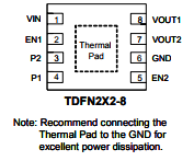
CXSD62459是一个双电源、低电流、低损耗的线性稳压器,采用节省空间的TDFN2X2-8封装。空载时的供电电流为100μA,在关断模式下,最大供电电流小于1μA,过流保护限值为430Ma。内置过热保护电路,防止热过载。

-
[ 产品资料下载 ]
目录
7.相关产品
产品概述 返回TOP
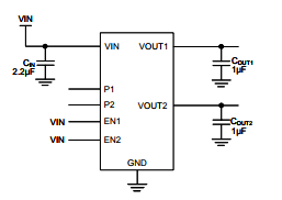
The CXSD62459 is a dual, low supply current, low dropout linear regulator that comes in a space saving TDFN2X2-8 package. The supply current at no-load is 100μA. In the shutdown mode, the maximum supply current is less than 1μA. The over-current protection limit is set at 430mA typical. An over-temperature protection circuit is built-in in the CXSD62459 to prevent thermal overload. These power saving features make the CXSD62459 ideal for use in the battery-powered applications such as notebook computers, cellular phones, and PDA’s. The GCXSD62459have two logic inputs that select one of nine preset output-voltage combinations, eliminating external 1% resistors. The GCXSD62459configures output voltages at VOUT1 and VOUT2 based on the state of P1 and P2 at power-on. Subsequent changes to P1 and P2 do not change the output voltages unless the supply power is cycled, or all EN inputs are simultaneously driven low to shut down the device. These devices feature a shutdown function and are offered in active low with auto discharge. The CXSD62459comes in a space saving TDFN2X2-8 package.
产品特点 返回TOP
„ Two Low-Dropout-Voltage Regulators
„ Pin-Programmable Output Voltages
„ 300mA Output Current for Each LDO
„ Independent Enable Control
„ Dropout Voltage is 90mV@ 100mA Load
„ Over-Temperature Protection and Short-Circuit Protection
„ Max. Supply Current in Shutdown Mode < 1μA
„ Small Ceramic Output Capacitors
应用范围 返回TOP
„ Notebook Computers
„ Cellular Phones
„ PDAs
„ Digital still Camera and Video Recorders
„ Hand-Held Devices
„ Bar Code Scanners
技术规格书(产品PDF) 返回TOP
需要详细的PDF规格书请扫一扫微信联系我们,还可以获得免费样品以及技术支持!

产品封装图 返回TOP

电路原理图 返回TOP
相关芯片选择指南 返回TOP 更多同类产品....
|
Dual Output |
||||||||||
|
Part NO. |
Vin(V min. |
Vin(V max. |
IOUT (A) |
VOUT (V) |
Dropout @IOUT(V |
EN |
Dis- charge |
IQ (μA) |
Note |
Package |
|
2.5 |
6 |
0.3 |
Programmable |
0.21 |
H |
Y |
85 |
MLCC |
TDFN2X2-8 |
|
|
2.5 |
6 |
0.3 |
VOUT1=1.8/2.5/2.8/ 2.85/3,VOUT2=1.8/ 2.8/2.85/3/3.3 |
0.21 |
H |
Y |
210 |
MLCC |
TSOT23-6/SOT23-6 TDFN2X2-8/TDFN3X3-8 |
|
|
2.5 |
6 |
0.3 |
VOUT1/2=1.8/2.5/ 2.8/3/3.3 |
0.21 |
H |
Y |
210 |
MLCC |
TSOT23-6 |
|
|
2.5 |
6 |
0.3 |
VOUT1=1.2/1.8/2.6/3 /3.3,VOUT2=1.8/2.85 /3.3 |
0.21 |
H |
Y |
60 |
MLCC |
WLCSP2X3-6/SOT-23-6 |
|
|
2.5 |
6 |
0.3 |
VOUT1=1.2~3.3 VOUT2=1.5~3.3 |
0.21 |
HPullLow |
Y |
60 |
MLCC |
TDFN1.6X1.6-6/TSOT-23-6/ADFN1.5X1.5-6 |
|
|
2.5 |
6 |
0.3 |
VOUT1=1.2~3.3 VOUT2=1.5~3.3 |
0.21 |
H |
Y |
60 |
MLCC |
TDFN1.6X1.6-6/TSOT-23-6/TDFN2X2-8 |
|
|
Special Functions |
||||||||||
|
Part NO. |
Vin(V min. |
Vin(V max. |
IOUT (A) |
VOUT (V) |
Dropout @IOUT(V |
EN |
Dis- charge |
IQ (μA) |
Note |
Package |
|
4.5 |
5.5 |
-- |
ADJ(0.5) |
-- |
H |
-- |
300 |
LDO driver |
SOT23-6 |
|
|
1.4 |
5.5 |
1 |
ADJ(0.8) |
0.125 |
H |
Y |
1000 |
MLCC,POK, Dual mode |
SOP8/SOP8(FD) |
|
|
1.4 |
5.5 |
2 |
ADJ(0.8) |
0.3 |
H |
Y |
1000 |
MLCC,POK, Dual mode |
SOP8/SOP8(FD) |
|
|
1.1 |
5.5 |
3 |
ADJ(0.8) |
0.38 |
H |
Y |
900 |
MLCC,POK,SS, Dual mode |
TSOT23-6/SOP8(FD)/ MSOP10(FD)/TDFN3X3-10 |
|
|
1.8 |
5.5 |
3 |
1.5 |
0.38 |
H |
Y |
900 |
MLCC,POK,SS |
TDFN3X3-10 |
|
|
1.1 |
5.5 |
3 |
ADJ(0.8) |
0.38 |
H |
Y |
900 |
MLCC,POK,SS, Dual mode |
TSOT23-6/SOP8(FD)/ MSOP10(FD)/TDFN3X3-10 |
|
|
1.1 |
5.5 |
3 |
ADJ(0.8) |
0.45 |
H |
Y |
1000 |
MLCC,POK |
SOP8(FD)/TDFN3X3-10 |
|
|
1.1 |
5.5 |
5 |
ADJ(0.8) |
0.2 |
H |
Y |
400 |
MLCC,POK,SS |
SOP-8(FD) |
|
|
1.1 |
5.5 |
4 |
ADJ(0.8) |
0.33 |
H |
Y |
400 |
MLCC,POK,SS |
SOP-8(FD) |
|
|
1.1 |
5.5 |
4 |
ADJ(0.8) |
0.3 |
H |
Y |
400 |
MLCC,POK,SS |
SOP-8(FD) |
|
|
1.1 |
5.5 |
2 |
ADJ(0.8) |
0.26 |
H |
Y |
400 |
MLCC,POK,SS, Dual mode |
SOP-8(FD) |
|
|
1 |
3.5 |
7 |
ADJ(0.8) |
0.138 |
H |
Y |
400 |
MLCC,POK,SS |
SOP8(FD) |
|
|
1 |
3.5 |
6 |
0.9/0.80/0.725/ 0.675/0.9/0.85/ 0.775/0.750 |
0.15 |
H |
Y |
400 |
VCCSA Power D0&D1&EN |
SOP8(FD) |
|
| 推荐信息 |
|---|
| 头条信息 |
|---|


