CXSD61022A wide input voltage, high efficiency CC step-down DC/DC converter that operates in either
| 产品型号: | CXSD61022A |
| 产品类型: | DC-DC转换器 |
| 产品系列: | Buck降压型芯片 |
| 产品状态: | 量产 |
| 浏览次数: | 64 次 |
产品简介
技术参数
| 输入电压范围 (VIN) | 42V |
|---|---|
| 输出电压 (VOUT) | 可调输出/带CC/cv模式 恒流模式保护 |
| 输出电流 (IOUT) | 2.5A |
| 工作频率 | 125K |
| 转换效率 | 94% |
| 封装类型 | TO-252-5L |
| Topology | Buck降压型芯片 |
| Control method | PWM/PFM |
| Switching frequency | 125K |
| Protection | 过流/过压/过温 |
| Features | 静态工作电流:3mA |
| Operating temp | -40℃~125℃ |
| Reference design | 反馈电压:0.8V |
产品详细介绍
目录
1.产品概述 2.产品特点
3.应用范围 4.产品封装图
5.电路原理图 6.产品PCB
7.产品BOM 8.产品PDF文档
9.功能概述 10.相关产品
一,产品概述(General Description)
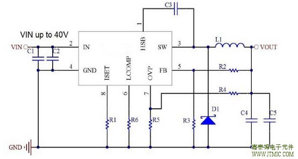
CXSD61022A is a wide input voltage, high efficiency CC step-down DC/DC converter that operates in either CV (Constant Output Voltage) mode or CC (Constant Output Current) mode. CXSD61022A provides up to 2.5A output current at 125kHz switching frequency.
CXSD61022A provides OVP pin for output over voltage protection.Protection features include cycle-by-cycle current limit,thermal shutdown, and frequency foldback at short circuit. The devices are available in a SOP-8EP package and require very few external devices for operation.
二.产品特点(Features)
42V Input Voltage Surge
40V Steady State Operation
Up to 2.5A output current
Output Voltage 2.5V to 10V
Resistor Programmable
− Current Limit from 1A to 2.5A
− Cable Compensation from 0Ω to 0.4Ω
±7.5% CC Accuracy
− Compensation of Input /Output Voltage Change
− Temperature Compensation
2% Feedback Voltage Accuracy
Up to 94% Efficiency
125kHz Switching Frequency Eases EMI Design
Advanced Feature Set
− Integrated Soft Start
− Thermal Shutdown
− Protection Against Shorted ISET Pin
Patented E-LTI technology improves
transient response.
SOP-8EP Package
三,应用范围 (Applications)
Car Charger/ Adaptor
Rechargeable Portable Devices
General-Purpose CC/CV Supply
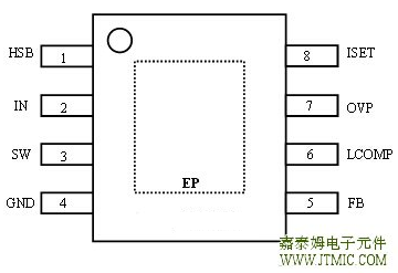
四,产品封装图 (Package)
|
Pin |
NAME |
Description |
|
1 |
HSB |
High Side Bias Pin. This provides power to the internal high-side MOSFET gate driver.Connect a 100nF capacitor from HSB pin to SW pin. |
|
2 |
IN |
Power Supply Input. Bypass this pin with a 10μF ceramic capacitor to GND, placed as close to the IC as possible. |
|
3 |
SW |
Power Switching Output to External Inductor. |
|
4 |
GND |
Ground. Connect this pin to a large PCB copper area for best heat dissipation. Return FB,COMP, and ISET to this GND, and connect this GND to power GND at a single point for best noise immunity. |
|
5 |
FB |
Feedback Input. The voltage at this pin is regulated to 0.800V. Connect to the resistor divider between output and GND to set the output voltage. |
|
6 |
LCOMP |
Output cable resistance compensation. |
|
7 |
OVP/EN |
CXSD61022A: OVP input. If the voltage at this pin exceeds 1.25V, the IC shuts down high-side switch.CXSD61022B: EN input. If the voltage at this pin is below 1.5V, the IC remains shut-off. |
|
8 |
ISET |
Output Current Setting Pin. Connect a resistor from ISET to GND to program the out putcurrent. |
|
Exposed |
Heat Dissipation Pad. Connect this exposed pad to large ground copper area with copper and vias. |
需要详细的PDF规格书请扫一扫微信联系我们,还可以获得免费样品以及技术支持!

九,功能概述
CV/CC Loop Regulation
As seen in Functional Block Diagram, the CXSD61022A is
a Constant On Time (COT) mode pulse width
modulation (PWM) converter with CC and CV control.
The converter operates as follows:
The main loop of CXSD61022A uses a COT mode control
which provides a very fast transient response with no
external component and no need loop compensation.
The CXSD61022A also adopt a proprietary circuit that
ensures enable use very low ESR capacitor to maintain
loop stability.
turns on. The high side MOSFET is turn off after
internal one shot timer expires. This one shot time is
set by VIN and VOUT to maintain a constant frequency.
The one shot timer is reset and high side MOSFET
turns on again when feedback voltage falls below the
reference voltage. An internal ramp is generating to
simulate output ripple, eliminating the need for ESR
induced output ripple from COT control mode. When
high side MOSFET turns off, the SW node of the
inductor swings to a diode voltage below ground,
causing the inductor current to decrease and magnetic
energy to be transferred to output. This state continues
until the next cycle start again
十,相关产品 更多同类产品......
|
DC-DC降压IC |
|||||||
|
型号 |
输入耐压 |
输出电压 |
输出电流 |
反馈电压 |
工作频率 |
效率 |
静态工作电流 |
|
42V |
可调输出/带CC/cv模式 恒流模式保护 |
3.5A |
0.8V |
125K |
94% |
3mA |
|
|
42V |
可调输出/带CC/cv模式 恒流模式保护 |
3A |
0.8V |
125K |
94% |
3mA |
|
|
42V |
可调输出/带CC/cv模式 恒流模式保护 |
2.5A |
0.8V |
125K |
94% |
3mA |
|
|
40V |
可调输出/带CC/cv模式 |
3A |
0.8V |
225K |
92% |
2.84mA |
|
|
50V |
5V固定输出 |
3.2A |
150K |
87% |
4.7mA |
||
|
50V |
5V固定输出 |
2.4A |
150K |
89% |
4.7mA |
||
|
50V |
5V固定输出 |
2.1A |
150K |
90% |
4.7mA |
||
|
50V |
5V固定输出 |
1.8A |
150K |
90% |
4.7mA |
||
|
40V |
可调输出/带CC/CV模式带线损补偿 |
3A |
0.8V |
125K |
94% |
4mA |
|
|
40V |
5V固定输出 |
3.5A |
150K |
93% |
2mA |
||
|
45V |
可调输出/ |
2A |
1.23V |
150K |
93% |
2mA |
|
|
40V |
可调输出/带CC/CV模式 |
2A |
1.18V |
110K |
93% |
10mA |
|
|
42V |
可调输出 |
3A |
0.8V |
50-500K |
91% |
3mA |
|
|
40V |
可调输出/带CC/cv模式 |
3A |
1.25V |
180K |
89% |
2.1mA |
|
|
40V |
可调输出/带CC/cv模式 |
3.5A |
1.25V |
180K |
87% |
2.1mA |
|
|
45V |
可调输出/带CC模式 |
3A |
1.25V |
150K |
89% |
2.0mA |
|
|
45V |
可调输出/带CC模式 |
2A |
1.235V |
150K |
83% |
2.0mA |
|
|
4.75V-40V |
可调输出 |
0.8A |
0.8V |
550K |
90% |
10uA |
|
|
4.0-42V |
可调输出 |
1.5A |
0.8V |
650K |
91% |
600uA |
|
|
4.5-25V |
可调输出 |
1.8A |
0.8V |
1.4M |
92% |
1.8mA |
|
|
20V |
可调输出 |
3.5A |
1.2V |
400K |
89% |
700uA |
|
|
28V |
可调输出 |
3A |
1.22V |
380K |
89% |
3mA |
|
|
20V |
可调输出 |
3A |
0.8V |
380K |
88% |
3mA |
|
|
20V |
可调输出 |
2A |
0.8V |
380K |
89% |
2mA |
|
|
45V |
5.0V/可调输出/3.3/12V |
2A |
1.23V |
150K |
82% |
2mA |
|
|
45V |
5.0V/可调输出 |
3A |
1.23V |
380K |
73% |
2mA |
|
|
27V |
可调输出 |
2A |
1.22V |
420K |
95% |
1mA |
|

 中文
中文 English

用户评论