 中文
中文 English
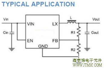
CXSD61038 high-efficiency high frequency synchronous step-down DC-DC regulator ICs capable of delivering up to 1.5A output currents Inrush Current Limit and Soft Start
| 产品型号: | CXSD61038 |
| 产品类型: | DC-DC转换器 |
| 产品系列: | Buck降压型芯片 |
| 产品状态: | 量产 |
| 浏览次数: | 60 次 |
产品简介
integrate main switch and synchronous switch with very low RDS(ON) to minimize
the conduction loss.It is ideal for powering portable equipment that runs from a
single cell Lithium-Ion (Li+) battery.
技术参数
| 输入电压范围 (VIN) | 2.0-6.0V |
|---|---|
| 输出电压 (VOUT) | 可调输出 |
| 输出电流 (IOUT) | 1.0A |
| 工作频率 | 1.5M |
| 转换效率 | 96% |
| 封装类型 | SOT-25 |
| Topology | Buck降压型芯片 |
| Control method | PWM/PFM |
| Switching frequency | 1.5M |
| Protection | 过流/过压/过温 |
| Features | 静态工作电流:20uA |
| Application | 待机电流:1uA |
| Operating temp | -40℃~125℃ |
| Reference design | 反馈电压:0.6V |
产品详细介绍
目录
1.产品概述 2.产品特点
3.应用范围 4.下载产品资料PDF文档
5.产品封装图 6.电路原理图
7.功能概述 8.相关产品
一,产品概述(General Description)
The CXSD61038 are high-efficiency, high frequency synchronous step-down
DC-DC regulator ICs capable of delivering up to 1.5A output currents. TheCXSD61038 can operate over a wide input voltage range from 2.3V to 5.5V and
integrate main switch and synchronous switch with very low RDS(ON) to minimize
the conduction loss.It is ideal for powering portable equipment that runs from a
single cell Lithium-Ion (Li+) battery. The output voltage can be regulated as low as
0.6V. The CXSD61038 can also run at 100% duty cycle for low dropout operation,
extending battery life in portable system.This device offers two operation modes,
PWM control and PFM Mode switchingcontrol, which allows a high efficiency over
the wider range of the load.
The CXSD61038 is offered in a low profile (1mm)5-pin, thin SOT package, and
is available in an adjustable version.
二.产品特点(Features)
1.)CXSD61038A 1.2A output current
2.)CXSD61038B 1.5A output current
3.)High Efficiency: Up to 96%
4.)1.5MHz Constant Frequency Operation
5.)No Schottky Diode Required
6.)2.3V to 5.5V Input Voltage Range
7.) Output Voltage as Low as 0.6V
8.)100% Duty Cycle in Dropout
9.) Low Quiescent Current: 35μA
10.)Slope Compensated Current Mode Control for Excellent Line
and Load Transient Response
11.)Short Circuit Protection
12.) Thermal Fault Protection
13.) Inrush Current Limit and Soft Start
14.)<1μA Shutdown Current
15.) Tiny SOT23-5 Package
三,应用范围 (Applications)
Cellular and Smart Phones
Wireless and DSL Modems
PDA
Digital Still and Video Cameras
MP3 Players
四.下载产品资料PDF文档
需要详细的PDF规格书请扫一扫微信联系我们,还可以获得免费样品以及技术支持!

五,产品封装图 (Package)
|
PIN |
NAME |
FUNCTION |
|
1 |
RUN |
Chip Enable Pin. Drive RUN above 1.5V to turn on the part. Drive |
|
2 |
GND |
Ground Pin |
|
3 |
SW |
Power Switch Output. It is the switch node connection to Inductor. |
|
4 |
VIN |
Power Supply Input. Must be closely decoupled to GND with a 10μF or greater ceramic capacitor. |
|
5 |
VOUT |
Output Voltage Feedback Pin. An internal resistive divider divides the |
六.电路原理图
七,功能概述
FUNCTIONAL DESCRIPTION
CXSD61038 is a synchronous buck regulator IC that integrates the PWM/PFM control, top
and bottom switches on the same die to minimize the switching transition loss and
conduction loss. With ultra low RDS(ON) power switches and proprietary PWM control,
this regulator IC can achieve the highest efficiency and the highest switch frequency
simultaneously to minimize the external inductor and capacitor size, and thus
achieving the minimum solution footprint.The CXSD61038 requires only three external
power components (Cin, Cout and L). Theadjustable version can be programmed
with external feedback to any voltage,ranging from 0.6V to the input voltage.
At dropout, the converter duty cycle increases to 100% and the output voltage
tracks the input voltage minus the Rdson drop of the high-side MOSFET.
The internal error amplifier and compensation provides excellent transient response, load,
and line regulation. Soft start function prevents input inrush current and output
overshoot during start up.
Inductor Selection
For most designs, the CXSD61038 operates with inductors of 1μH to 4.7μH. Low inductance
values are physically smaller but require faster switching, which results in some efficiency loss.
The inductor value can be derived from the following equation:
L =VIN × ∆I L × f OSC
Where ∆I L is inductor Ripple Current. Large value inductors result in lower ripple current and
small value inductors result in high ripple current. For optimum voltage-positioning load
transients, choose an inductor with DC series resistance in the 50mΩ to 150mΩ range.
Input Capacitor Selection
With the maximum load current at 1.5A, the maximum ripple current through input capacitor
is about 0.6Arms. A typical X7R or better grade ceramic capacitor with 6V rating and greater
than 10uF capacitance can handle this ripple current well. To minimize the potential noise
problem, place this ceramic capacitor really close to the IN and
GND pins. Care should be taken to minimizethe loop area formed by CIN, and IN/GND pins.
Output Capacitor Selection
The output capacitor is required to keep the output voltage ripple small and to ensure
regulation loop stability. The output capacitor must have low impedance at the switching
frequency. Ceramic capacitors with X5R or X7R dielectrics are recommended due to their low
ESR and high ripple current ratings. The outputripple VOUT is determined by:
VOUT × (V IN − VOUT ) 1
V IN × f OSC × L 8 × f osc × C3
A 10μF ceramic can satisfy most applications.PC Board Layout Checklist When laying out the printed
circuit board, the following checking should be used to ensure proper operation of the CXSD61038. Check the
following in your layout:
1. The power traces, consisting of the GND trace, the SW trace and the VIN traceshould be kept short,
direct and wide.
2. Does the (+) plates of Cin connect to Vin as closely as possible? This capacitor provides the AC current
to the internal power MOSFETs.
3. Keep the switching node, SW, away from the sensitive VOUT node.
4. Keep the (-) plates of Cin and Cout as close as possible
八,相关产品 更多同类产品......
|
低压同步DC-DC降压IC |
|||||||||
|
型号 |
输入耐压 |
输出电压 |
输出电流 |
反馈电压 |
工作频率 |
效率 |
静态工作电流 |
待机电流 |
封装 |
|
2.0-6.0V |
1.2V/1.8V/3.3V/可调输出 |
0.7A |
0.6V |
1.5MHz |
96% |
20uA |
SOT-25 |
||
|
2.5-6.0V |
可调输出 |
1A |
0.6V |
1.5MHz |
96% |
20uA |
SOT-25 |
||
|
2.0-6.0V |
可调输出 |
1.0A |
0.6V |
1.5M |
96% |
20uA |
1uA |
SOT-25 |
|
|
2.3-6.0V |
可调输出 |
1.2A |
0.6V |
1.5M |
96% |
35uA |
1uA |
SOT-25 |
|
|
2.3-6.0V |
可调输出 |
1.5A |
0.6V |
1.5M |
96% |
35uA |
1uA |
SOT-25 |
|
|
2.3-6.0V |
可调输出 |
1.5A |
0.6V |
1.5M |
96% |
35uA |
1uA |
SOT-25 |
|
|
2.0-6.5V |
可调输出 |
2.0A |
0.6V |
1.5M |
96% |
40uA |
1uA |
SOT-26 |
|
|
2.6-6.0V |
可调输出 |
2.0A |
0.6V |
3M |
96% |
30uA |
0.1uA |
SOT-25 |
|
|
2.3-6.5V |
可调输出 |
2.0A |
0.6V |
1.5M |
96% |
40uA |
40uA |
SOP-8 |
|
|
2.3-6.5V |
可调输出 |
3.0A |
0.6V |
1.5M |
95% |
40uA |
40uA |
ESOP-8 |
|
|
2.3V-6.5V |
可调输出 |
1.3A |
0.6V |
1.5M |
96% |
35uA |
35uA |
DFN2*2-6 |
|
|
2.3V-6.5V |
可调输出 |
2A |
0.6V |
1.5M |
95% |
40uA |
40uA |
DFN3*3-10 |
|

用户评论