 中文
中文 English
CXSD6253 380KHz fixed frequency PWM buck (step-down) DC/DC converter capable of driving a 2A load with high efficiency
目录
1.产品概述 2.产品特点 3.应用范围 4.技术规格书下载(产品PDF文档)
5.产品封装图 6.电路原理图 7.功能概述 8.相关产品
一,产品概述(General Description) ![]()
The CXSD6253 is a 380KHz fixed frequency PWM buck (step-down)
DC/DC converter,capable of driving a 2A load with high efficiency, low ripple
and excellent line and load regulation. Requiring a minimum number of external components, the regulator is simple to use and include internal frequency compensation and a fixed-frequency oscillator.
The PWM control circuit is able to adjust the duty ratio linearly from 0 to 100%. An enable function, an over current protection function is built inside. When short protection function happens, the operation frequency will be reduced from 380KHz to 80KHz. An internal compensation block is built in to minimize external component count.
二.产品特点(Features)![]()
Wide 3.6V to 18V Input Voltage Range
Output Adjustable from 1.222V to 16V
Maximum Duty Cycle 100%
Minimum Drop Out 0.6V
Fixed 380KHz Switching Frequency
2A Constant Output Current Capability
Internal Optimize Power MOSFET
High efficiency
Excellent line and load regulation
TTL shutdown capability
EN pin with hysteresis function
Built in thermal shutdown function
Built in current limit function
Built in output short protection function
Available in SOP8L package
三,应用范围 (Applications)![]()
LCD Monitor and LCD TV
Digital Photo Frame
Set-up Box
ADSL Modem
Telecom / Networking Equipment
四.技术规格书下载(产品PDF)![]()
需要详细的PDF规格书请扫一扫微信联系我们,还可以获得免费样品以及技术支持!

五,产品封装图 (Package)![]()

|
Pin Number |
Pin Name |
Description |
|
1,6,8 |
NC |
No Connected. |
|
2 |
VIN |
Supply Voltage Input Pin. CXSD6253 operates from a 3.6V to 18V |
|
3 |
SW |
Power Switch Output Pin (SW). Output is the switch node that |
|
4 |
GND |
Ground Pin. Care must be taken in layout. This pin should be |
|
5 |
FB |
Feedback Pin (FB). Through an external resistor divider |
|
7 |
EN |
Enable Pin. Drive EN pin low to turn off the device, drive it |
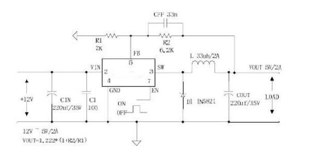
六.电路原理图![]()

七,功能概述![]()
|
Parameter |
Symbol |
Value |
Unit |
|
Input Voltage |
Vin |
-0.3 to 20 |
V |
|
Feedback Pin Voltage |
VFB |
-0.3 to Vin |
V |
|
EN Pin Voltage |
VEN |
-0.3 to Vin |
V |
|
Output Switch Pin Voltage |
VOutput |
-0.3 to Vin |
V |
|
Power Dissipation |
PD |
Internally limited |
mW |
|
Thermal Resistance (SOP8) |
RJA |
100 |
oC/W |
|
Operating Junction Temperature |
TJ |
-40 to 125 |
oC |
|
Storage Temperature |
TSTG |
-65 to 150 |
oC |
|
Lead Temperature (Soldering, 10 sec) |
TLEAD |
260 |
oC |
|
ESD (HBM) |
2000 |
V |
八.DEMO BOARD MANUAL
(一)CXSD6253 典型应用测试:
|
参数 |
符号 |
值 |
单位 |
|
输入电压 |
VIN |
3.6 to 18 |
V |
|
输出电压 |
VOUT |
5 |
V |
|
输出电流 |
IOUT |
0 to 2 |
A |
1. CXSD6253 12V 转 5V(负载 0.2A—2A)应用电路图:
2. CXSD6253 12V 转 5V(负载 0.2A—2A)效率图和输出电压变化曲线:
(二)CXSD6253 PCB 板布局建议:
(1)流大电流的线要粗,短,不拐弯。
(2)4 脚(GND),2 脚(VIN)线要粗,短线,不拐弯,且输入电解电容 CIN 和 105 C1 陶
瓷电容紧挨第 2 脚(VIN)和 4 脚(GND)。(主要是为了减小输入电源布线寄生的电感,电阻
产生的高压开关毛刺干扰)
(3)3 脚(SW)输出线要粗,短线,不拐弯,电感和续流二极管要紧挨第 3 脚(SW)输出端。
(4)5 脚(FB)走线要接到输出滤波电容 C2,COUT 之后, PCB 布线远离 L1,D1,避免噪声干扰。
CXSD6253PCB 图: (三)CXSD6253 温度测试数据:
1:CXSD6253 电路图和 PCB 版图。

2:CXSD6253 DEMO 板工作时(12V 转 5V)各元件温度,自然通风,室温:16℃。
|
输出负载电流 |
0.2A |
0.5A |
1A |
1.5A |
2A |
|
27℃ |
28℃ |
31℃ |
33℃ |
42℃ |
|
|
电感(33uH/2A) |
24℃ |
25℃ |
28℃ |
29℃ |
35℃ |
|
肖特基二极管(IN5822) |
22℃ |
25℃ |
26℃ |
30℃ |
35℃ |
|
输入电容(35V/220uF) |
22℃ |
23℃ |
25℃ |
26℃ |
31℃ |
|
输出电容(35V/220uF) |
22℃ |
23℃ |
24℃ |
26℃ |
29℃ |
八,相关芯片选择指南![]()
|
降压型直流电源变换器芯片(高效率型) |
|||||
|
产品型号 |
输入电压 |
开关电流 |
开关频率 |
电压版本 |
封装类型 |
|
3.6V ~ 18V |
2A |
380KHz |
Adj (1.222V) |
SOP8L |
|
|
3.6V ~ 23V |
3A |
380KHz |
Adj (1.222V) |
SOP8L |
|
|
3.6V ~ 18V |
2A |
380KHz |
Adj (0.8V) |
SOP8L |
|
|
3.6V ~ 18V |
3A |
380KHz |
Adj (0.8V) |
SOP8L |
|


发表评论