 中文
中文 English
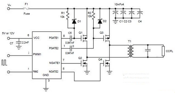
CXSD6290全桥配置中驱动两个高侧P通道和两个低侧N通道mosfet输出由PWM1和PWM2输入独立控制
目录
1.产品概述 2.产品特点
3.应用范围 4.下载产品资料PDF文档
5.产品封装图 6.电路原理图
7.功能概述 8.相关产品
一,产品概述(General Description)
The CXSD6290 is designed to drive two high-side P-chan-nel
MOSFETs and two low-side N-channel MOSFETs in a full-bridge
configuration. The outputs are independently controlled by PWM1
and PWM2 input signals.The other features include VCC power-
on-reset and ther-mal shutdown.
二.产品特点(Features)
1.)Wide Input Voltage Range: 4.5V to 13.2V
2.)Drives a Full-Bridge Inverter(High-Side P-
3.)Channel MOSFETs and Low-Side N-Channel MOSFETs)
4.)Thermal Shutdown Protection
5.)VCC Power-On-Reset SOP-8 Package
6.)Lead Free and Green Devices Available
三,应用范围 (Applications)
LCD Monitor and LCD TV
四.下载产品资料PDF文档
需要详细的PDF规格书请扫一扫微信联系我们,还可以获得免费样品以及技术支持!

五,产品封装图 (Package)

FUNCTION
六.电路原理图

七,功能概述
Thermal Shutdown
shutdown circuit will pull PGATE outputs high and NGATE outputs low thus turning high-side and low-side
MOSFET off. When the driver cools down below 110ïC after a ther-mal shutdown, it resumes normal operation
and follows the PWM input signals.
Power-On-Reset (POR)
The CXSD6290 provides the power-on-reset function that keeps the driver disable when the VCC voltage
is insuffi-cient to driver external MOSFETs reliably. The PGATE out-puts remain high and the NGATE outputs
remain low until the VCC voltage exceeds POR threshold. Once the POR threshold is reached, the condition
of gate driver outputs is defined by the PWM signals.
Layout Consideration
In any high switching frequency application, a correct lay-out is important to ensure proper operation of the
device.With power devices switching at high frequency, the re-sulting current transient will cause voltage
spike across the interconnecting impedance and parasitic circuit elements. As an example, consider the
turn-off transition of the PWM MOSFET. Before turn-off, the MOSFET is car-rying the full load current. During
turn-off, current stops flowing in the MOSFET and is free-wheeling by the lower MOSFET and parasitic diode.
Any parasitic inductance of the circuit generates a large voltage spike during the switching interval. In general,
using short and wide printed circuit traces should minimize interconnecting imped-ances and the magnitude of
voltage spike. Below is a checklist for your layout :
- Keep the switching nodes (PGATE, NGATE and the drain of the MOSFETs) away from sensitive small sig-
nal nodes (PWM1, PWM2, MS, and DTC ) since these nodes are fast moving signals. Therefore, keep traces
to these nodes as short as possible.
- Place the drain of the P-MOSFET and the drain of the N-MOSFET as close as possible to minimize the imped
ance with wide layout plane between the two pads and reduce the voltage bounce of the node.
- The traces from the gate drivers to the MOSFETs (PGATE and NGATE) should be short and wide.
- The VCC decoupling capacitor (C7), C5, C6, and RDTC should be close to their pins.
- The input capacitor should be near the source of the P-MOSFET.
- The drain of the MOSFETs should be a large plane for heat sinking.
八,相关产品 更多同类产品......
|
Switching Regulator > Buck Controller |
||||||||||
|
Part_No |
Package |
Archi tectu |
Phase |
No.of PWM Output |
Output Current (A) |
Input Voltage (V) |
Reference Voltage (V) |
Bias Voltage (V) |
Quiescent Current (uA) |
|
|
min |
max |
|||||||||
|
SOP-14 QSOP-16 QFN4x4-16 |
VM |
1 |
1 |
30 |
2.9 |
13.2 |
0.9 |
12 |
8000 |
|
|
SOP-8 |
VM |
1 |
1 |
20 |
2.9 |
13.2 |
0.8 |
12 |
5000 |
|
|
SOP-8 |
VM |
1 |
1 |
20 |
2.9 |
13.2 |
0.8 |
12 |
5000 |
|
|
QFN4x4-24 |
VM |
2 |
1 |
60 |
3.1 |
13.2 |
0.6 |
12 |
5000 |
|
|
SOP-8 |
VM |
1 |
1 |
20 |
2.2 |
13.2 |
0.8 |
5~12 |
2100 |
|
|
SOP-8 |
VM |
1 |
1 |
20 |
2.2 |
13.2 |
0.8 |
5~12 |
2100 |
|
|
SOP8|TSSOP8 |
VM |
1 |
1 |
5 |
5 |
13.2 |
1.25|0.8 |
5~12 |
3000 |
|
|
SOP-8 |
VM |
1 |
1 |
10 |
3.3 |
5.5 |
0.8 |
5 |
2100 |
|
|
SOP-14 |
VM |
1 |
1 |
10 |
5 |
13.2 |
0.8 |
12 |
2000 |
|
|
TSSOP-24 |QFN5x5-32 |
VM |
1 |
2 |
20 |
5 |
13.2 |
0.6 |
5~12 |
4000 |
|
|
SOP14 QSOP16 QFN-16 |
VM |
1 |
1 |
30 |
2.9 |
13.2 |
0.9 |
12 |
4000 |
|
|
SOP-14 |
VM |
1 |
1 |
30 |
2.2 |
13.2 |
0.6 |
12 |
5000 |
|
|
SOP-14 |
VM |
1 |
1 |
30 |
2.2 |
13.2 |
0.6 |
12 |
5000 |
|
|
SOP-14 |
VM |
1 |
1 |
25 |
2.2 |
13.2 |
0.8 |
12 |
5000 |
|
|
LQFP7x7 48 TQFN7x7-48 |
VM |
1 |
6 |
0.015 |
1.4 |
6.5 |
- |
5 |
1800 |
|
|
TSSOP-24P |
VM |
1 |
2 |
20 |
2.97 |
5.5 |
0.8 |
5~12 |
5000 |
|
|
SOP-14 |
VM |
1 |
1 |
10 |
5 |
13.2 |
0.8 |
12 |
3000 |
|
|
SOP-8-P|DIP-8 |
VM |
1 |
1 |
30 |
2.9 |
13.2 |
1.2 |
12 |
3000 |
|
|
SSOP28 QFN4x4-24 |
VM |
1 |
2 |
20 |
5 |
24 |
0.9 |
5 |
1200 |
|
|
SOP-20 |
VM |
1 |
2 |
20 |
2.2 |
13.2 |
0.6 |
5~12 |
4000 |
|
|
SOP8|DFN3x3-10 |
VM |
1 |
2 |
- |
- |
- |
- |
5~12 |
550 |
|
|
DIP8|SOP-8 |
VM |
1 |
1 |
1 |
1.2 |
9 |
24 |
5 |
9 ~ 24 |
|
|
|
||||||||||


发表评论