 中文
中文 English
CXSD62108单相恒定时间同步的脉宽调制控制器驱动N通道mosfet笔记本电脑中产生低压芯片组RAM电源的电压
|
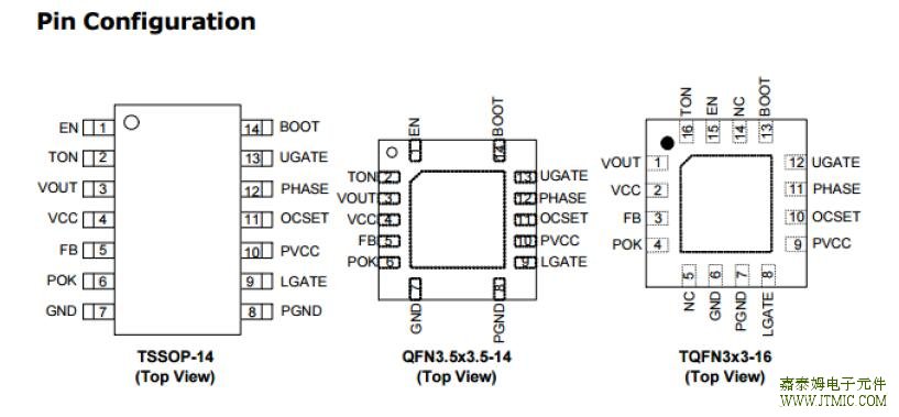
目录 1.产品概述 2.产品特点 一,产品概述(General Description) loading-modulated switching frequencies. In PWM Mode, the converter works nearly at constant frequency for low-noise requirements. internal integrated soft-start ramps up the output voltage with programmable slew rate to reduce the start-up current. A soft-stop function actively discharges the output capacitors. 需要详细的PDF规格书请扫一扫微信联系我们,还可以获得免费样品以及技术支持! 五,产品封装图 (Package) |


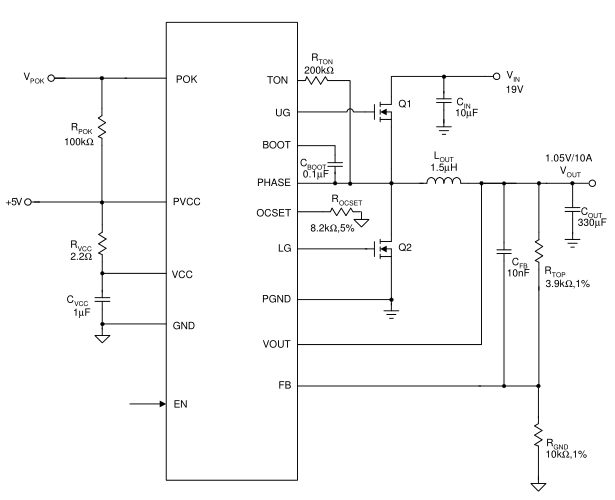
六.电路原理图

七,功能概述
Layout Consideration (Cont.)
· The signals going through theses traces have both high dv/dt and high di/dt with high peak charging and dis-
charging current. The traces from the gate drivers to the MOSFETs (UGATE and LGATE) should be short and wide.
· Place the source of the high-side MOSFET and the drain of the low-side MOSFET as close as possible. Minimiz-
ing the impedance with wide layout plane between the two pads reduces the voltage bounce of the node. In
addition, the large layout plane between the drain of the MOSFETs (VIN and PHASE nodes) can get better heat
sinking.
· The PGND is the current sensing circuit reference ground and also the power ground of the LGATE low-
side MOSFET. On the hand, the PGND trace should be a separate trace and independently go to the source of the
low-side MOSFET. Besides, the current sense resistor should be close to OCSET pin to avoid parasitic capaci-
tor effect and noise coupling.
· Decoupling capacitors, the resistor-divider, and boot capacitor should be close to their pins. (For example, place
the decoupling ceramic capacitor close to the drain of the high-side MOSFET as close as possible.)
· The input bulk capacitors should be close to the drain of the high-side MOSFET, and the output bulk capacitors
should be close to the loads. The input capacitor’s ground should be close to the grounds of the output capacitors
and low-side MOSFET.
· Locate the resistor-divider close to the FB pin to mini-mize the high impedance trace. In addition, FB pin traces
can’t be close to the switching signal traces (UGATE, LGATE, BOOT, and PHASE).
八,相关产品 更多同类产品......
|
Switching Regulator > Buck Controller |
||||||||||
|
Part_No |
Package |
Archi tectu |
Phase |
No.of PWM Output |
Output Current (A) |
Input Voltage (V) |
Reference Voltage (V) |
Bias Voltage (V) |
Quiescent Current (uA) |
|
|
min |
max |
|||||||||
|
SOP-14 QSOP-16 QFN4x4-16 |
VM |
1 |
1 |
30 |
2.9 |
13.2 |
0.9 |
12 |
8000 |
|
|
SOP-8 |
VM |
1 |
1 |
20 |
2.9 |
13.2 |
0.8 |
12 |
5000 |
|
|
SOP-8 |
VM |
1 |
1 |
20 |
2.9 |
13.2 |
0.8 |
12 |
5000 |
|
|
QFN4x4-24 |
VM |
2 |
1 |
60 |
3.1 |
13.2 |
0.6 |
12 |
5000 |
|
|
SOP-8 |
VM |
1 |
1 |
20 |
2.2 |
13.2 |
0.8 |
5~12 |
2100 |
|
|
SOP-8 |
VM |
1 |
1 |
20 |
2.2 |
13.2 |
0.8 |
5~12 |
2100 |
|
|
SOP8|TSSOP8 |
VM |
1 |
1 |
5 |
5 |
13.2 |
1.25|0.8 |
5~12 |
3000 |
|
|
SOP-8 |
VM |
1 |
1 |
10 |
3.3 |
5.5 |
0.8 |
5 |
2100 |
|
|
SOP-14 |
VM |
1 |
1 |
10 |
5 |
13.2 |
0.8 |
12 |
2000 |
|
|
TSSOP-24 |QFN5x5-32 |
VM |
1 |
2 |
20 |
5 |
13.2 |
0.6 |
5~12 |
4000 |
|
|
SOP14 QSOP16 QFN-16 |
VM |
1 |
1 |
30 |
2.9 |
13.2 |
0.9 |
12 |
4000 |
|
|
SOP-14 |
VM |
1 |
1 |
30 |
2.2 |
13.2 |
0.6 |
12 |
5000 |
|
|
SOP-14 |
VM |
1 |
1 |
30 |
2.2 |
13.2 |
0.6 |
12 |
5000 |
|
|
SOP-14 |
VM |
1 |
1 |
25 |
2.2 |
13.2 |
0.8 |
12 |
5000 |
|
|
LQFP7x7 48 TQFN7x7-48 |
VM |
1 |
6 |
0.015 |
1.4 |
6.5 |
- |
5 |
1800 |
|
|
TSSOP-24P |
VM |
1 |
2 |
20 |
2.97 |
5.5 |
0.8 |
5~12 |
5000 |
|
|
SOP-14 |
VM |
1 |
1 |
10 |
5 |
13.2 |
0.8 |
12 |
3000 |
|
|
SOP-8-P|DIP-8 |
VM |
1 |
1 |
30 |
2.9 |
13.2 |
1.2 |
12 |
3000 |
|
|
SSOP28 QFN4x4-24 |
VM |
1 |
2 |
20 |
5 |
24 |
0.9 |
5 |
1200 |
|
|
SOP-20 |
VM |
1 |
2 |
20 |
2.2 |
13.2 |
0.6 |
5~12 |
4000 |
|


发表评论