 中文
中文 English
CXSD6297电压模式固定300kHz开关频率同步降压变换器上电复位(POR)电路监测VCC电源电压以防止错误的逻辑控制
目录
1.产品概述 2.产品特点
3.应用范围 4.下载产品资料PDF文档
5.产品封装图 6.电路原理图
7.功能概述 8.相关产品
一,产品概述(General Description)
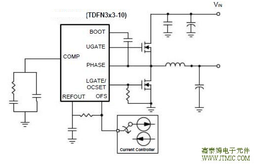
The CXSD6297 is a voltage mode, fixed 300kHz switching frequency, synchronous buck converter. The CXSD6297 allows wide input voltage that is either a single 5V~12V or two supply voltage(s) for various applications. The power-on-reset (POR) circuit monitors the VCC supply voltage to prevent wrong logic controls. A built-in soft-start circuit prevents the output voltages from overshoot as well as limits the input current. An internal 0.8V tempera-ture-compensated reference voltage with high accuracy is designed to meet the requirement of low output volt-age applications. The CXSD6297 provides excellent out-put voltage regulations against load current variation.CXSD6297 is built in reference voltage offset function for applications that require adjusting supply voltage.The controller’s over-current protection monitors the out-put current by using the voltage drop across the RDS(ON) of low-side MOSFET, eliminating the need for a current sens-ing resistor that features high efficiency and low cost. In addition, the CXSD6297 also integrates excellent protec-tion functions, The over-voltage protection (OVP) , under-voltage protection (UVP) and over-temperature protec-tion (OTP). OVP circuit which monitors the FB voltage to prevent the PWM output from over voltage, and UVP cir-cuit which monitors the FB voltage to prevent the PWM output from under voltage or short circuit. OTP circuit which
monitors the junction temperature to prevent over-heat-ing conditions.
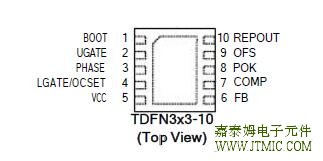
The CXSD6297 is available in TDFN3x3-10 package
二.产品特点(Features)
1.)Wide 5V to 12V Supply Voltage
2.)Power-On-Reset Monitoring on VCC
3.)Excellent Output Voltage Regulations
- 0.8V Internal Reference
- ±1% Over Temperature Range
4.)Integrated Soft-Start
5.)Voltage Mode PWM Operation with External Compensation
6.)Up to 90% Duty Ratio for Fast Transient Response
7.)Constant Switching Frequency
- 300kHz ±10%
8.)Integrated Bootstrap Forward P-CH MOSFET
9.)Drive Dual Low Cost N-MOSFETs with Adaptive Dead Time Control
10.)50% Under-Voltage Protection
11.)125% Over-Voltage Protection
12.)Adjustable Over-Current Protection Threshold
- Using the RDS(ON) of Low-Side MOSFET
13.)Shutdown Control by COMP
14.)Power Good Monitoring
15.)TDFN3x3-10 Package
16.)Lead Free and Green Devices Available (RoHS Compliant)
三,应用范围 (Applications)
Graphic Cards
DSL, Switch HUB
Wireless Lan
Notebook Computer
Mother Board
LCD Monitor/TV
四.下载产品资料PDF文档
需要详细的PDF规格书请扫一扫微信联系我们,还可以获得免费样品以及技术支持!

五,产品封装图 (Package)

六.电路原理图

七,功能概述
Layout Consideration
In any high switching frequency converter, a correct lay-out is important to ensure proper operation of the
regulator. With power devices switching at 300kHz,the resulting current transient will cause voltage spike across
the interconnecting impedance and parasitic circuit elements. As an example, consider the turn-off transition
of the PWM MOSFET. Before turn-off, the MOSFET is car-rying the full load current. During turn-off, current stops
flowing in the MOSFET and is free-wheeling by the lower MOSFET and parasitic diode. Any parasitic inductance of
the circuit generates a large voltage spike during the switching interval. In general, using short and wide printed
circuit traces should minimize interconnecting imped
Layout Consideration (Cont.)
ances and the magnitude of voltage spike. And signal and power grounds are to be kept separate till combined
using ground plane construction or single point grounding. Figure 8. illustrates the layout, with bold lines
indicating high current paths; these traces must be short and wide. Components along the bold lines should be
placed lose together. Below is a checklist for your layout:
- Keep the switching nodes (UGATE, LGATE, and PHASE) away from sensitive small signal nodes since these
nodes are fast moving signals. Therefore, keep traces to these nodes as short as possible.
The traces from the gate drivers to the MOSFETs (UG and LG) should be short and wide.
- Place the source of the high-side MOSFET and the drain of the low-side MOSFET as close as possible. Minimiz-
ing the impedance with wide layout plane between the two pads reduces the voltage bounce of the node.
Decoupling capacitor, compensation component, the resistor dividers, and boot capacitors should be close
their pins. (For example, place the decoupling ceramic capacitor near the drain of the high-side MOSFET as
close as possible. The bulk capacitors are also placed near the drain).
- The input capacitor should be near the drain of the up-per MOSFET; the output capacitor should be near the
loads. The input capacitor GND should be close to the output capacitor GND and the lower MOSFET GND.
- The drain of the MOSFETs (VIN and PHASE nodes) should be a large plane for heat sinking.
The ROCSET resistance should be placed near the IC as close as possible.
八,相关产品 更多同类产品......
|
Switching Regulator > Buck Controller |
||||||||||
|
Part_No |
Package |
Archi tectu |
Phase |
No.of PWM Output |
Output Current (A) |
Input Voltage (V) |
Reference Voltage (V) |
Bias Voltage (V) |
Quiescent Current (uA) |
|
|
min |
max |
|||||||||
|
SOP-14 QSOP-16 QFN4x4-16 |
VM |
1 |
1 |
30 |
2.9 |
13.2 |
0.9 |
12 |
8000 |
|
|
SOP-8 |
VM |
1 |
1 |
20 |
2.9 |
13.2 |
0.8 |
12 |
5000 |
|
|
SOP-8 |
VM |
1 |
1 |
20 |
2.9 |
13.2 |
0.8 |
12 |
5000 |
|
|
QFN4x4-24 |
VM |
2 |
1 |
60 |
3.1 |
13.2 |
0.6 |
12 |
5000 |
|
|
SOP-8 |
VM |
1 |
1 |
20 |
2.2 |
13.2 |
0.8 |
5~12 |
2100 |
|
|
SOP-8 |
VM |
1 |
1 |
20 |
2.2 |
13.2 |
0.8 |
5~12 |
2100 |
|
|
SOP8|TSSOP8 |
VM |
1 |
1 |
5 |
5 |
13.2 |
1.25|0.8 |
5~12 |
3000 |
|
|
SOP-8 |
VM |
1 |
1 |
10 |
3.3 |
5.5 |
0.8 |
5 |
2100 |
|
|
SOP-14 |
VM |
1 |
1 |
10 |
5 |
13.2 |
0.8 |
12 |
2000 |
|
|
TSSOP-24 |QFN5x5-32 |
VM |
1 |
2 |
20 |
5 |
13.2 |
0.6 |
5~12 |
4000 |
|
|
SOP14 QSOP16 QFN-16 |
VM |
1 |
1 |
30 |
2.9 |
13.2 |
0.9 |
12 |
4000 |
|
|
SOP-14 |
VM |
1 |
1 |
30 |
2.2 |
13.2 |
0.6 |
12 |
5000 |
|
|
SOP-14 |
VM |
1 |
1 |
30 |
2.2 |
13.2 |
0.6 |
12 |
5000 |
|
|
SOP-14 |
VM |
1 |
1 |
25 |
2.2 |
13.2 |
0.8 |
12 |
5000 |
|
|
LQFP7x7 48 TQFN7x7-48 |
VM |
1 |
6 |
0.015 |
1.4 |
6.5 |
- |
5 |
1800 |
|
|
TSSOP-24P |
VM |
1 |
2 |
20 |
2.97 |
5.5 |
0.8 |
5~12 |
5000 |
|
|
SOP-14 |
VM |
1 |
1 |
10 |
5 |
13.2 |
0.8 |
12 |
3000 |
|
|
SOP-8-P|DIP-8 |
VM |
1 |
1 |
30 |
2.9 |
13.2 |
1.2 |
12 |
3000 |
|
|
SSOP28 QFN4x4-24 |
VM |
1 |
2 |
20 |
5 |
24 |
0.9 |
5 |
1200 |
|
|
SOP-20 </ |
||||||||||


发表评论