 中文
中文 English
CXSD6289两个同步降压型脉宽调制控制器脉冲宽度调制控制器设计用于同步驱动两个N通道mosfet buck拓扑
目录
1.产品概述 2.产品特点
3.应用范围 4.下载产品资料PDF文档
5.产品封装图 6.电路原理图
7.功能概述 8.相关产品
一,产品概述(General Description)
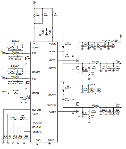
The CXSD6289 has two synchronous buck PWM control-lers with high
precision internal references voltage to of-fer accurate outputs. The PWM
controllers are designed to drive two N-channel MOSFETs in synchronous
buck topology. The device requires 12V and 5V power supplies.If the 5V
supply is not available, the device can offer an optional shunt regulator
5.8V for 5V supply.Both outputs have independent soft-start and enable
func-tions combined on the SS/EN pin. Connecting a capaci-tor from each
SS/EN pin to the ground for setting the soft-start time, and pulling the SS/EN
pin voltage below 1V to disable regulator. The device also offers 180°phase
shift function between OUT1 and OUT2.The default switching frequency is
300kHz (keep the FS pin open or short to GND), and the device also provides
the programmable switching frequency function to ad-just the switching frequency
from 70kHz to 800kHz. Con-necting a resistor from FS pin to GND increases the
switching frequency. Conversely, connecting a resistor from FS pin to VCC12
decreases the switching frequency.There is no current sensing or under-voltage
sensing on the CXSD6289. However, it provides a simple short-circuit protection by monitoring the COMP1 pin and COMP2 pin for over-voltage. When any of two pins
exceed their trip point and the condition keeps for 1-2 internal clock cycles (3-6us at
300kHz), all regulators are latched off.
二.产品特点(Features)
1.)Two Synchronous Buck Converters(OUT1,OUT2)
2.)Converter Input Voltage Range up to 12V
3.)0.6V Reference for OUT1 with 0.8% Accuracy
4.)3.3V Reference for OUT2 with 0.8% Accuracy
5.)Both Outputs have Independent Soft-Start and
Enable Functions
6.)Internal 300kHz Oscillator and Programmable
Frequency Range from 70 kHz to 800kHz
7.)180 Degrees Phase Shift etween OUT1 and OUT2
8.)Short-Circuit Protection
9.)Thermally Enhanced SOP-20 Package
10.)Lead Free and Green Devices Available
(RoHS Compliant)
三,应用范围 (Applications)
Graphic Cards
Low-Voltage Distributed Power Supplies
SMPS Application
四.下载产品资料PDF文档
需要详细的PDF规格书请扫一扫微信联系我们,还可以获得免费样品以及技术支持!

五,产品封装图 (Package)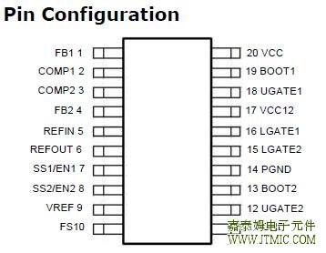

六.电路原理图

七,功能概述
Output Inductor Selection (Cont.)
Where Fs is the switching frequency of the regulator. Al-though increase the inductor value and frequency
reduce the ripple current and voltage, but there is a tradeoff ex-ists between the inductor’s ripple current and
the regula-tor load transient response time.A smaller inductor will give the regulator a faster load transient
response at the expense of higher ripple current.Increasing the switching frequency (FS) also reduces the
ripple current and voltage, but it will increase the switch-ing loss of the MOSFET and the power dissipation
of the converter. The maximum ripple current occurs at the maximum input voltage. A good starting point is
to choose the ripple current to be approximately 30% of the maxi-mum output current.Once the inductance
value has been chosen, select an inductor that is capable of carrying the required peak cur-rent without going
into saturation. In some types of inductors, especially core that is made of ferrite, the ripple current will increase
abruptly when it saturates. This will result in a larger output ripple voltage.
Output Capacitor Selection
Higher Capacitor value and lower ESR reduce the output ripple and the load transient drop. Therefore select high
performance low ESR capacitors that are intended for switching regulator applications. In some applications,
multiple capacitors have to be parallel to achieve the de-sired ESR value. A small decoupling capacitor in parallel
for bypassing the noise is also recommended, and the voltage rating of the output capacitors are also must be
considered. If tantalum capacitors are used, make sure they are surge tested by the manufactures. If in doubt,
consult the capacitors manufacturer.
Input Capacitor Selection
The input capacitor is chosen based on the voltage rating and the RMS current rating. For reliable operation,
select the capacitor voltage rating to be at least 1.3 times higher than the maximum input voltage.
The maximum RMS current rating requirement is approxi-mately IOUT/2, where IOUT is the load current.
During power up, the input capacitors have to handle large amount of surge current. If tantalum capacitors
are used, make sure they are surge tested by the manufactures. If in doubt, consult the capacitors
manufacturer. For high frequency decoupling, a ceramic capacitor 1uF can be connected between the
drain of upper MOSFET and the source of lower MOSFET.
MOSFET Selection
The selection of the N-channel power MOSFETs are de-termined by the RDS(ON), reverse transfer
capacitance (CRSS) and maximum output current requirement. The losses in the MOSFETs have
two components: conduction loss and transition loss. For the upper and lower MOSFET, the
losses are approximately given by the following :
PUPPER=IOUT(1+TC)(RDS(ON))D+(0.5)(IOUT)(VIN)(tSW)FS
PLOWER=IOUT(1+TC)(RDS(ON))(1-D)
Where I is the load current OUT TC is the temperature dependency of RDS(ON) F is the switching
frequency St is the switching interval sw D is the duty cycle Note that both MOSFETs have
conduction losses while the upper MOSFET include an additional transition loss.The switching
internal, tsw, is a function of the reverse transfer capacitance CRSS. The (1+TC) term is to
factor in the temperature depen-dency of the RDS(ON) and can be extracted from the “RDS(ON)
vs Temperature” curve of the power MOSFET.
Short Circuit Protection
The CXSD6289 provides a simple short circuit protection function, and it is not easy to predict its
performance, since many factors can affect how well it works. Therefore, the limitations and
suggestions of this method must be pro-vided for users to understand how to work it well.The
short circuit protection was not designed to work for the output in initial short condition. In this
case, the short circuit protection may not work, and damage the MOSFETs. If the circuit still works,
remove the short can cause an inductive kick on the phase pin, and it may damage the IC and
MOSFETs. If the resistance of the short is not low enough to cause protection, the regulator will
work as the load has
Short Circuit Protection (Cont.)
increased, and continue to regulate up until the MOSFETs is damaged. The resistance of the short
should include wiring, PCB traces, contact resistances, and all of the return paths.The higher duty
cycle will give a higher COMP voltage level, and it is easy to touch the trip point. The compensa-
tion components also affect the response of COMP voltage; smaller caps may give a faster response.
The output current has faster rising time during short;the COMP pin will have a sharp rise. However,
if the cur-rent rises too fast, it may cause a false trip. The output capacitance and its ESR can affect
the rising time of the current during short.
八,相关产品 更多同类产品......
|
Switching Regulator > Buck Controller |
||||||||||
|
Part_No |
Package |
Archi tectu |
Phase |
No.of PWM Output |
Output Current (A) |
Input Voltage (V) |
Reference Voltage (V) |
Bias Voltage (V) |
Quiescent Current (uA) |
|
|
min |
max |
|||||||||
|
SOP-14 QSOP-16 QFN4x4-16 |
VM |
1 |
1 |
30 |
2.9 |
13.2 |
0.9 |
12 |
8000 |
|
|
SOP-8 |
VM |
1 |
1 |
20 |
2.9 |
13.2 |
0.8 |
12 |
5000 |
|
|
SOP-8 |
VM |
1 |
1 |
20 |
2.9 |
13.2 |
0.8 |
12 |
5000 |
|
|
QFN4x4-24 |
VM |
2 |
1 |
60 |
3.1 |
13.2 |
0.6 |
12 |
5000 |
|
|
SOP-8 |
VM |
1 |
1 |
20 |
2.2 |
13.2 |
0.8 |
5~12 |
2100 |
|
|
SOP-8 |
VM |
1 |
1 |
20 |
2.2 |
13.2 |
0.8 |
5~12 |
2100 |
|
|
SOP8|TSSOP8 |
VM |
1 |
1 |
5 |
5 |
13.2 |
1.25|0.8 |
5~12 |
3000 |
|
|
SOP-8 |
VM |
1 |
1 |
10 |
3.3 |
5.5 |
0.8 |
5 |
2100 |
|
|
SOP-14 |
VM |
1 |
1 |
10 |
5 |
13.2 |
0.8 |
12 |
2000 |
|
|
TSSOP-24 |QFN5x5-32 |
VM |
1 |
2 |
20 |
5 |
13.2 |
0.6 |
5~12 |
4000 |
|
|
SOP14 QSOP16 QFN-16 |
VM |
1 |
1 |
30 |
2.9 |
13.2 |
0.9 |
12 |
4000 |
|
|
SOP-14 |
VM |
1 |
1 |
30 |
2.2 |
13.2 |
0.6 |
12 |
5000 |
|
|
SOP-14 |
VM |
1 |
1 |
30 |
2.2 |
13.2 |
0.6 |
12 |
5000 |
|
|
SOP-14 |
VM |
1 |
1 |
25 |
2.2 |
13.2 |
0.8 |
12 |
5000 |
|
|
LQFP7x7 48 TQFN7x7-48 |
VM |
1 |
6 |
0.015 |
1.4 |
6.5 |
- |
5 |
1800 |
|
|
TSSOP-24P |
VM |
1 |
2 |
20 |
2.97 |
5.5 |
0.8 |
5~12 |
5000 |
|
|
SOP-14 |
VM |
1 |
1 |
10 |
5 |
13.2 |
0.8 |
12 |
3000 |
|
|
SOP-8-P|DIP-8 |
||||||||||


发表评论