 中文
中文 English
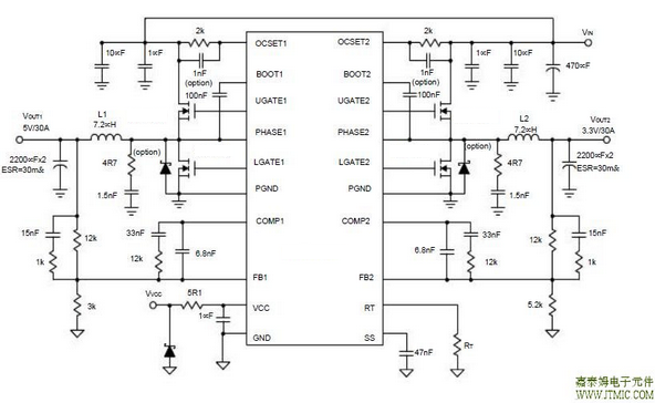
CXSD62117双通道电压模式和同步PWM控制器驱动双N通道mosfet两个通道均采用180度相移
|
目录 1.产品概述 2.产品特点3.应用范围 4.下载产品资料PDF文档 5.产品封装图 6.电路原理图 7.功能概述 8.相关产品 一,产品概述(General Description) Protection (UVP) and Over-Voltage Protection (OVP) moni-tor the FB 二.产品特点(Features) 四.下载产品资料PDF文档 需要详细的PDF规格书请扫一扫微信联系我们,还可以获得免费样品以及技术支持!
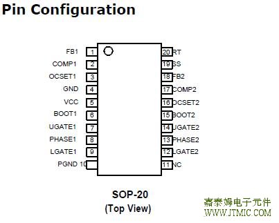
五,产品封装图 (Package)
六.电路原理图
七,功能概述 |


Layout Consideration
In any high switching frequency converter, a correct lay-out is important to ensure proper operation of the
regulator. With power devices switching at 200kHz, the resulting current transient will cause voltage spike across the interconnecting impedance and parasitic circuit elements. As an example, consider the turn-off transition of the PWM MOSFET. Before turn-off, the MOSFET is car-rying the full load current. During turn-off, current stops flowing in the MOSFET and is free-wheeling by the lower MOSFET and parasitic diode. Any parasitic inductance of the circuit generates a large voltage spike during the switching interval. In general, using short and wide printed circuit traces should minimize interconnecting imped- ances and the magnitude of voltage spike. And signal and power grounds are to be kept separating till com-bined using the ground plane construction or single point grounding. Figure 8. illustrates the layout, with bold lines
Layout Consideration (Cont.)
indicating high current paths; these traces must be short and wide. Components along the bold lines should be
placed lose together. Below is a checklist for your layout:- Keep the switching nodes (UGATE, LGATE, and PHASE)away from sensitive small signal nodes since these nodes are fast moving signals. Therefore, keep traces
to these nodes as short as possible.
- The traces from the gate drivers to the MOSFETs (UGATEand LGATE) should be short and wide.
- Place the source of the high-side MOSFET and the drainof the low-side MOSFET as close as possible. Minimiz-ing the impedance with wide layout plane between the two pads reduces the voltage bounce of the node.
- Decoupling capacitor, compensation component, the resistor dividers, and boot capacitors should be close
their pins. (For example, place the decoupling ceramic capacitor near the drain of the high-side MOSFET as
close as possible. The bulk capacitors are also placed near the drain).
- The input capacitor should be near the drain of the up-per MOSFET; the output capacitor should be near the
loads. The input capacitor GND should be close to the lower MOSFET GND.
- The drain of the MOSFETs (VIN and PHASE nodes)should be a large plane for heat sinking.
- The ROCSET resistance should be placed near the IC as close as possible.
- The decoupling capacitor for VCC should be placed near the VCC and GND. CBOOT should be connected as
close to the BOOT and PHASE pins as possible.
八,相关产品 更多同类产品......
|
Switching Regulator > Buck Controller |
||||||||||
|
Part_No |
Package |
Archi tectu |
Phase |
No.of PWM Output |
Output Current (A) |
Input Voltage (V) |
Reference Voltage (V) |
Bias Voltage (V) |
Quiescent Current (uA) |
|
|
min |
max |
|||||||||
|
SOP-14 QSOP-16 QFN4x4-16 |
VM |
1 |
1 |
30 |
2.9 |
13.2 |
0.9 |
12 |
8000 |
|
|
SOP-8 |
VM |
1 |
1 |
20 |
2.9 |
13.2 |
0.8 |
12 |
5000 |
|
|
SOP-8 |
VM |
1 |
1 |
20 |
2.9 |
13.2 |
0.8 |
12 |
5000 |
|
|
QFN4x4-24 |
VM |
2 |
1 |
60 |
3.1 |
13.2 |
0.6 |
12 |
5000 |
|
|
SOP-8 |
VM |
1 |
1 |
20 |
2.2 |
13.2 |
0.8 |
5~12 |
2100 |
|
|
SOP-8 |
VM |
1 |
1 |
20 |
2.2 |
13.2 |
0.8 |
5~12 |
2100 |
|
|
SOP8|TSSOP8 |
VM |
1 |
1 |
5 |
5 |
13.2 |
1.25|0.8 |
5~12 |
3000 |
|
|
SOP-8 |
VM |
1 |
1 |
10 |
3.3 |
5.5 |
0.8 |
5 |
2100 |
|
|
SOP-14 |
VM |
1 |
1 |
10 |
5 |
13.2 |
0.8 |
12 |
2000 |
|
|
TSSOP-24 |QFN5x5-32 |
VM |
1 |
2 |
20 |
5 |
13.2 |
0.6 |
5~12 |
4000 |
|
|
SOP14 QSOP16 QFN-16 |
VM |
1 |
1 |
30 |
2.9 |
13.2 |
0.9 |
12 |
4000 |
|
|
SOP-14 |
VM |
1 |
1 |
30 |
2.2 |
13.2 |
0.6 |
12 |
5000 |
|
|
SOP-14 |
VM |
1 |
1 |
30 |
2.2 |
13.2 |
0.6 |
12 |
5000 |
|
|
SOP-14 |
VM |
1 |
1 |
25 |
2.2 |
13.2 |
0.8 |
12 |
5000 |
|
|
LQFP7x7 48 TQFN7x7-48 |
VM |
1 |
6 |
0.015 |
1.4 |
6.5 |
- |
5 |
1800 |
|
|
TSSOP-24P |
VM |
1 |
2 |
20 |
2.97 |
5.5 |
0.8 |
5~12 |
5000 |
|
|
SOP-14 |
VM |
1 |
1 |
10 |
5 |
13.2 |
0.8 |
12 |
3000 |
|
|
SOP-8-P|DIP-8 |
VM |
1 |
1 |
30 |
2.9 |
13.2 |
1.2 |
12 |
3000 |
|
|
SSOP28 QFN4x4-24 |
VM |
1 |
2 |
20 |
5 |
24 |
0.9 |
5 |
1200 |
|
|
SOP-20 |
VM |
1 |
2 |
20 |
2.2 |
13.2 |
0.6 |
5~12 |
4000 |
|
|
SOP8|DFN3x3-10 |
VM |
1 |
2 |
- |
- |
|||||


发表评论