 中文
中文 English
5A同步降压转换器CXSD62122 50mΩ P沟道功率MOSFET和20mΩ N沟道功率MOSFET电流模式控制方案
目录
1.产品概述 2.产品特点
3.应用范围 4.下载产品资料PDF文档
5.产品封装图 6.电路原理图
7.功能概述 8.相关产品
一,产品概述(General Description)
The CXSD62122 is a 5A, synchronous, step-down converter with integrated 50mΩ P-channel power MOSFET and 20mΩ N-channel power MOSFET.The device, with cur-rent-mode control scheme, can convert 4.5~26V input volt-age to the output voltage adjustable from 0.8 to 90% VIN to provide excellent output voltage regulation.
The CXSD62122 regulates the output voltage in an auto-matic PSM/PWM mode operation, depending on the out-put current, for high efficiency operation over light to full load current. The CXSD62122 is also equipped with power-
on-reset, soft-start, and whole protections (including over- voltage, under-voltage, over-temperature, and current-limit) in a single package. In shutdown mode, the supply current drops below 5μA.This device, available in 28-pin TQFN5x6 package, pro-vides a very compact system solution with minimal exter-
nal components and good thermal conductance.
二.产品特点(Features)
Wide Input Voltage from 4.5V to 26V
Output Current Up to 5A
Adjustable Output Voltage from 0.8V to 90%VIN
- 0.8V Reference Voltage
- ±2.5% System Accuracy
Integrated 50mΩ P-Channel Power MOSFET and
20mΩ N-Channel Power MOSFET
High Efficiency up to 95%
Current-Mode Operation
- Stable with Ceramic Output Capacitors
- Fast Transient Response
Power-On-Reset Monitoring
Fixed 380kHz Switching Frequency in PWM Mode
Automatic Pulse-Skipping Mode (PSM)/PWM
Mode Operation
Built-in Digital Soft-Start
Output Current-Limit Protection with Frequency
Foldback
·70% Under-Voltage Protection
·Over-Temperature Protection
·118% Over-Voltage Protection
·<5μA Quiescent Current During Shutdown
·Thermal-Enhanced TQFN5x6-28 Package
·Pb-Free Available as an Option
·Lead Free and Green Devices Available
(RoHS Compliant)
三,应用范围 (Applications)
LCD Monitor / TV
SetTop Box
Portable DVD
Wireless LAN
ADSL, Switch HUB
Notebook Computer
Step-Down Converters Requiring High Efficiency
and 5A Output Current
四.下载产品资料PDF文档
需要详细的PDF规格书请扫一扫微信联系我们,还可以获得免费样品以及技术支持!

五,产品封装图 (Package)

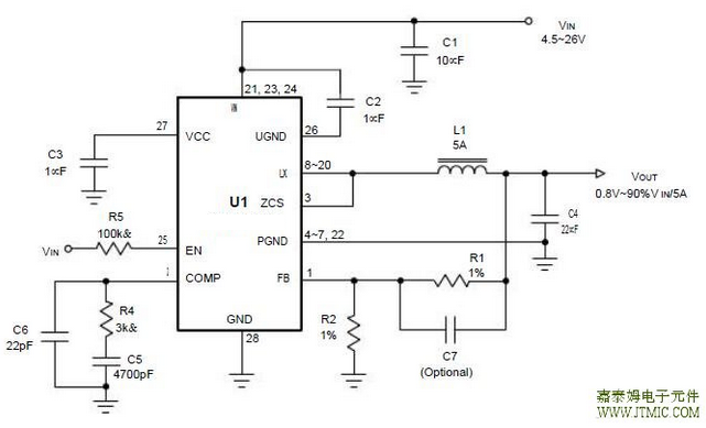
六.电路原理图

七,功能概述
Inductor Value Calculation
The operating frequency and inductor selection are inter-related in that higher operating frequencies permit
the use of a smaller inductor for the same amount of inductor ripple current. However, this is at the expense
of efficiency due to an increase in MOSFET gate charge losses. The equation (2) shows that the inductance
value has a direct effect on ripple current.Accepting larger values of ripple current allows the use of low
inductances, but results in higher output voltage ripple
Layout Consideration
In high power switching regulator, a correct layout is im-portant to ensure proper operation of the regulator.
In general, interconnecting impedance should be minimized by using short, wide printed circuit traces. Signal
and power grounds are to be kept separating and finally com-bined using ground plane construction or single
point grounding. Figure 2 illustrates the layout, with bold lines indicating high current paths. Components
along the bold lines should be placed close together. The following is a checklist for your layout:
1. Firstly, to initial the layout by placing the power components. Orient the power circuitry to achieve a clean
power flow path. If possible, make all the connections on one side of the PCB with wide, copper filled areas.
2. In Figure 2, the loops with the same color bold lines conduct high slew rate current. These interconnecting
impedances should be minimized by using wide, short printed circuit traces.
3. Keep the sensitive small signal nodes (FB, COMP) away from switching nodes (LX or others) on the PCB.
Therefore, place the feedback divider and the feedback compensation network close to the IC to avoid switching
noise. Connect the ground of feedback divider directly to the GND pin of the IC using a dedicated ground trace.
4. The VCC decoupling capacitor should be right next to the VCC and GND pins. Capacitor C2 should be connected
as close to the VIN and UGND pins as possible.
5. Place the decoupling ceramic capacitor C1 near the VIN as close as possible. The bulk capacitors C8 are also
placed near VIN. Use a wide power ground plane to con- nect the C1, C8, and C4 to provide a low impedance
八,相关产品 更多同类产品.......
|
Switching Regulator > Buck Converter |
|||||||||||
|
Part_No |
Package |
Architectu |
No.of PWM Outpu |
Drive Lout (A) |
Vin(V) |
Fmax Khz |
Vref (V) |
R-Top (milohm) |
R-Sync (milohm) |
Iq (No load) (uA) |
|
|
min |
max |
||||||||||
|
TQFN5x6-28 |
CM |
1 |
5 |
4.5 |
26 |
380 |
0.8 |
50 |
20 |
1000 |
|
|
SOP-8 |
CM |
1 |
2 |
4.5 |
26 |
380 |
0.8 |
100 |
1000 |
||
|
SOP-8P |
CM |
1 |
4 |
4.5 |
26 |
380 |
0.8 |
80 |
1000 |
||
|
SOT23-5|TSOT23-5 |
CM |
1 |
1 |
2.7 |
6 |
1500 |
0.6 |
280 |
250 |
25 |
|
|
SOT23-5 |
CM |
1 |
1 |
2.7 |
6 |
1500 |
0.6 |
280 |
250 |
||
|
SOP-8 |
CM |
1 |
3 |
4.3 |
14 |
500 |
0.8 |
70 |
70 |
500 |
|
|
SOP-8P |
CM |
1 |
3 |
4.3 |
14 |
500 |
0.8 |
55 |
45 |
500 |
|
|
TDFN3x3-10 |
3 |
2.6 |
5.5 |
2000 |
0.8 |
110 |
110 |
460 |
|||
|
TDFN3x3-10 |
CM |
2 |
1 |
2.7 |
6 |
1500 |
0.6 |
280 |
250 |
500 |
|
|
TDFN3x3-10 |
CM |
2 |
1 |
2.7 |
6 |
1500 |
0.6 |
280 |
250 |
||
|
TDFN2x2-6 |
CM |
1 |
1 |
2.7 |
6 |
1500 |
0.6 |
280 |
250 |
25 |
|
|
TDFN2x2-6 |
CM |
1 |
1 |
2.7 |
6 |
1500 |
0.6 |
280 |
250 |
||
|
TDFN3x3-12 |
CM |
2 |
1 |
2.7 |
6 |
1500 |
0.6 |
280 |
250 |
25 |
|
|
TDFN3x3-12 |
CM |
2 |
1 |
2.7 |
6 |
1500 |
0.6 |
280 |
250 |
||
|
TDFN 3x3 12 |
CM |
2 |
1 |
3 |
5.5 |
1500 |
0.6 |
280 |
250 |
30 |
|
|
TQFN3x3-20 |
CM |
3 |
2 |
2.9 |
5.5 |
1500 |
0.6 |
- |
- |
300 |
|
|
TDFN2x2-8 |
CM |
1 |
1 |
3.3 |
8 |
1500 |
0.6 |
280 |
250 |
25 |
|
|
SOP-8 |
CM |
1 |
2 |
4.5 |
24 |
340 |
0.925 |
110 |
110 |
1900 |
|
|
SOP-8P |
CM |
1 |
3 |
4.5 |
24 |
340 |
0.925 |
110 |
110 |
1900 |
|
|
|
|||||||||||


发表评论