 中文
中文 English
2.6V至6.5V输入电源VGON和VGOFF的线性调节器控制器CXSU63137电流模式升压调节器大电流运算放大器
目录
1.产品概述 2.产品特点
3.应用范围 4.下载产品资料PDF文档
5.产品封装图 6.电路原理图
7.功能概述 8.相关产品
一,产品概述(General Description)
The CXSU63137 integrates with a high-performance step-up converter, two linear-regulator controllers, a high voltage switch and one (CXSU63137), three (CXSU63137) or five (CXSU63137) high current operational amplifiers for TFT-LCD applications.The main step-up regulator is a current-mode, fixed-fre-quency PWM switching regulator. The 1.2MHz switching frequency allows the usage of low-profile inductors and ceramic capacitors to minimize the thickness of LCD panel designs.
The linear-regulator controllers used external transistors provide regulated the gate-driver of TFT-LCD VGON and VGOFF supplies.
The amplifiers are ideal for VCOM and VGAMMA applications, with
150m A peak output current drive, 10MHz bandwidth, and 13V/μs slew
rate. All inputs and outputs are rail-to-rail.
The CXSU63137/1/2 is available in a tiny 5mm x 5mm 32-pin QFN package (TQFN5x5-32).
二.产品特点(Features)
· 2.6V to 6.5V Input Supply Range
· Current-Mode Step-Up Regulator
- Fast Transient Response
- 1.2MHz Fixed Operating Frequency
· ±1.5% High-Accuracy Output Voltage
· 3A, 20V, 0.25W Internal N-Channel MOSFET
· High Efficiency
· Low Quiescent Current (0.6mA Typical)
· Linear-Regulator Controllers for VGON and VGOFF
· High-performance Operational Amplifiers
- ±150mA Output Short-Circuit Current
- 13V/ms Slew Rate - 10MHz, -3dB Bandwidth
- Rail-to-Rail Inputs/Outputs
· Fault-Delay Timer and Fault Latch for All Regulator Outputs
· Over-Temperature Protection
· Available in Compact 32-pin 5mmx5mm Thin QFN Package (TQFN5x5-32)
· Lead Free Available (RoHS Compliant)
三,应用范围 (Applications)
TFT LCD Displays for Monitors
TFT LCD Displays for Notebook Computers
Automotive Displays
四.下载产品资料PDF文档
需要详细的PDF规格书请扫一扫微信联系我们,还可以获得免费样品以及技术支持!

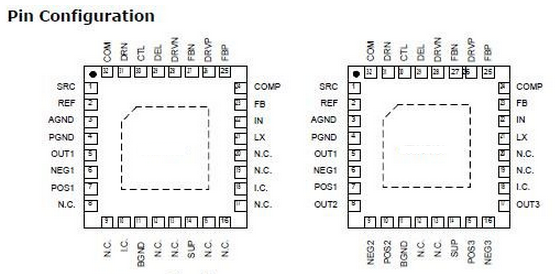
五,产品封装图 (Package)

 Pin Function Description
|
Pin |
Name |
Function Description |
||
|
CXSU63137 |
CXSU63137-1 |
CXSU63137-2 |
||
|
1 |
SRC |
SRC |
SRC |
Switch Input. Source of the internal high-voltage P-channel MOSFET. Bypass |
|
2 |
REF |
REF |
REF |
Reference voltage output. Bypass REF to AGND with a minimum of |
|
3 |
AGND |
AGND |
AGND |
Analog Ground for Step-Up Regulator and Linear Regulators. Connect to |
|
4 |
PGND |
PGND |
PGND |
Power Ground for Step-Up Regulator. PGND is the source of the main step-up |
|
5 |
OUT1 |
OUT1 |
OUT1 |
Output of Operational-Amplifier 1 |
|
6 |
NEG1 |
NEG1 |
NEG1 |
Inverting Input of Operational-Amplifier 1 |
|
7 |
POS1 |
POS1 |
POS1 |
Non-inverting Input of Operational-Amplifier 1 |
|
8 |
NC |
OUT2 |
OUT2 |
Output of Operational-Amplifier 2 of CXSU63137/CXSU63137. No internal |
|
9 |
NC |
NEG2 |
NEG2 |
Inverting Input of Operational-Amplifier 2 of CXSU63137/CXSU63137. No internal |
|
10 |
IC |
POS2 |
POS2 |
Non-inverting Input of Operational-Amplifier 2 of CXSU63137/CXSU63137. Internal |
|
11 |
BGND |
BGND |
BGND |
Analog Ground for Operational Amplifiers. Connect to power ground (PGND) |
|
12 |
NC |
NC |
POS3 |
Non-inverting Input of Operational-Amplifier 3 of CXSU63137. No internal |
|
13 |
NC |
NC |
OUT3 |
Output of Operational-Amplifier 3 of CXSU63137. No internal connected ofCXSU63137/CXSU63137. |
|
14 |
SUP |
SUP |
SUP |
Power Input of Operational Amplifiers. Typically connected to VMAIN. Bypass |
|
15 |
NC |
POS3 |
POS4 |
Non-inverting Input of Operational-Amplifier 4 of CXSU63137. Non-inverting |
|
16 |
NC |
NEG3 |
NEG4 |
Inverting Input of Operational-Amplifier 4 of CXSU63137. Inverting Input of |
|
17 |
NC |
OUT3 |
OUT4 |
Output of Operational-Amplifier 4 of CXSU63137. Output of |
|
18 |
IC |
IC |
POS5 |
Non-inverting Input of Operational-Amplifier 5 of CXSU63137. Internal connected |
|
19 |
NC |
NC |
NEG5 |
Inverting Input of Operational-Amplifier 5 of CXSU63137. No internal connected |
|
20 |
NC |
NC |
OUT5 |
Output of Operational-Amplifier 5 of CXSU63137. No internal connected ofCXSU63137/CXSU63137. |
|
21 |
LX |
LX |
LX |
N-Channel Power MOSFET Drain and Switching Node. Connect the inductor |
|
22 |
IN |
IN |
IN |
Supply Voltage Input. Bypass IN to AGND with a 0.1μF capacitor. IN can range |
|
23 |
FB |
FB |
FB |
Step-Up Regulator Feedback Input. Connect a resistive voltage-divider from |
|
24 |
COMP |
COMP |
COMP |
Step-Up Regulator Error-Amplifier Compensation Point. Connect a series RC |
PinFunction Description
|
Pin |
Name |
Function Description |
||
|
CXSU63137 |
CXSU63137-1 |
CXSU63137-2 |
||
|
24 |
COMP |
COMP |
COMP |
Step-Up Regulator Error-Amplifier Compensation Point. Connect a series RC |
|
25 |
FBP |
FBP |
FBP |
Gate-On Linear-Regulator Feedback Input. Connect FBP to the center of a |
|
26 |
DRVP |
DRVP |
DRVP |
Gate-On Linear-Regulator Base Drive. Open drain of an internal n-channel |
|
27 |
FBN |
FBN |
FBN |
Gate-Off Linear-Regulator Feedback Input. Connect FBN to the center of a |
|
28 |
DRVN |
DRVN |
DRVN |
Gate-Off Linear-Regulator Base Drive. Open drain of an internal p-channel |
|
29 |
DEL |
DEL |
DEL |
High-Voltage Switch Delay Input. Connect a capacitor from DEL to AGND to |
|
30 |
CTL |
CTL |
CTL |
High-Voltage Switch Control Input. When CTL is high, the high-voltage switch |
|
31 |
DRN |
DRN |
DRN |
Switch Input. Drain of the internal high-voltage back-to-back P-channel |
|
32 |
COM |
COM |
COM |
Internal High-Voltage MOSFET Switch Common Terminal. Do not allow the |
六.电路原理图
七,功能概述
For all switching power supplies, the layout is an impor-tant step in the design; especially at high peak currents and switching frequencies. There are some general guidelines for layout:
1.Place the external power components (the input capacitors, output capacitors, boost inductor and output diodes, etc.) in close proximity to the device.Traces to these components should be kept as short and wide as possible to minimize parasitic inductance and resistance.
2.Place the REF and IN bypass capacitors close to the pins. The ground connection of the IN bypass capacitor should be connected directly to the AGND pin with a wide trace.
3.Create a power ground (PGND) and a signal ground island and connect at only one point. The power ground consisting of the input and output capacitor grounds, PGND pin, and any charge-pump components. Connect all of these together with short, wide traces or a small ground plane. Maxi-mizing the width of the power ground traces im-proves efficiency and reduces output voltage ripple and noise spikes. The analog ground plane (AGND) consisting of the AGND pin, all the feed-back-divider ground connections, the operational-amplifier divider ground connections, the COMP and DEL capacitor ground connections, and the device’s exposed backside pad. Connect the AGND and PGND islands by connecting the PGND pin directly to the exposed backside pad. Make no other connections between these separate ground planes.
4.The feedback network should sense the output volt-age directly from the point of load, and be as far away from LX node as possible.
5.The exposed die plate, underneath the package,should be soldered to an equivalent area of metal on the PCB. This contact area should have mul-tiple via connections to the back of the PCB as well as connections to intermediate PCB layers, if available, to maximize thermal dissipation away from the IC.
6.To minimize the thermal resistance of the package when soldered to a multi-layer PCB, the amount of copper track and ground plane area connected to the exposed die plate should be maximized and spread out as far as possible from the IC. The bot-tom and top PCB areas especially should be maxi-mized to allow thermal dissipation to the surround-ing air.
7.Minimize feedback input track lengths to avoid switching noise pick-up
八,相关产品
|
Switching Regulator > Boost Converter |
|||||||||||
|
Part_No |
Package |
Archi-tecture |
Input Voltage |
Max Adj. Output Voltage |
Switch Current Limit (max) |
Fixed Output Voltage |
Switching Frequency |
Internal Power Switch |
Sync. Rectifier |
||
|
min |
max |
min |
max |
(A) |
(V) |
(kHz) |
|||||
|
SOT89 |
VM |
0.9 |
5.5 |
2.5 |
5.5 |
0.5 |
1.8|2.6|2.8|3 |3.3|3.8|4.5|5 |
- |
No |
Yes |
|
|
MSOP8|TSSOP8 |SOP8 |
VM |
2.5 |
5.5 |
2.5 |
- |
- |
- |
200 ~ 1000 |
No |
No |
|
|
TSSOP8|SOP-8P |
VM |
1 |
5.5 |
2.5 |
5 |
1 |
2.5|3.3 |
300 |
Yes |
Yes |
|
|
SOP8 |
CM |
3 |
40 |
1.25 |
40 |
1.5 |
- |
33 ~ 100 |
Yes |
No |
|
|
TQFN5x5-32 |
CM |
2.5 |
6.5 |
2.5 |
18 |
3 |
No |
1200 |
Yes |
No |
|
|
TSOT23-5 TDFN2x2-6 |
CM |
2.5 |
6 |
2.5 |
20 |
2 |
- |
1500 |
Yes |
No |
|
|
TQFN4x4-6 TDFN3x3-12 |
CM |
1.8 |
5.5 |
2.7 |
5.5 |
5 |
- |
1.2 |
Yes |
Yes |
|
|
SOT23-5 |
CM |
2.5 |
6 |
2.5 |
32 |
1 |
- |
1000 |
Yes |
No |
|
|
TSOT-23-6 TDFN2x2-8 |
CM |
1.2 |
5.5 |
1.8 |
5.5 |
1.2 |
- |
1.2 |
Yes |
Yes |
|


发表评论